Enabling the Smart, Connected Factory

At Cimetrix Incorporated, our mission is "Enabling the Smart, Connected Factory." We support high-technology manufacturing in the semiconductor, photovoltaic, LED, and other industries by making factory equipment smarter, allowing them to communicate with host factory systems, and delivering decision-making tools. Our focus is to support our customers as they work to increase productivity, reduce costs, and improve quality.

To be successful in this mission, we invest in the development of new software products, but also by participating in the SEMI and ISMI industry consortiums.

With the proliferation of SEMI standards, more industries — such as LEDs, flat panel displays (FPD), disk drives, and surface mount technology (SMT) assembly — recognize they can reduce costs and improve quality by levering off of the common knowledge in the industry.

We offer the following information as background on the industries we support.

Semiconductors

Semiconductor Front End

  • Implant
  • Deposition
  • Etch
  • Patterning
  • Metrology

Chips - also known as semiconductor devices - are integrated circuits we all use for every electronic device or subsystem. Semiconductor device fabrication is a multi-step sequence of photolithographic and chemical processing steps during which electronic circuits are gradually created on a wafer typically made of ultra-pure silicon, but sometimes different compound semiconductors are used for very specialize applications. The entire manufacturing process takes many weeks and is performed in highly specialized facilities referred to as fabs.

The cost of building and setting up a semiconductor fabrication facility ("fab") is expensive, estimated about $1 billion for a new fab, and over $3 billion for one of today's most advanced semiconductor fabs.

The central part of a fab is the clean room, an area where the environment is controlled to eliminate all dust, since even a single speck can ruin a microcircuit, which has features much smaller than dust. The clean room must also be dampened against vibration and the fab needs to maintain a very narrow range of temperature and humidity. Controlling temperature and humidity is critical for minimizing static electricity.

Wafers are thin (~0.75mm) and typically round, and the most advanced fabs today develop chips on 300mm wafers, about the size of a dinner plate. While these wafers may not look that expensive, their value, when eventually turned into integrated circuits, represent over $30,000 each and can be worth as much as a $1 million, if not more. Because of the value of these wafers, semiconductor fabs need to make sure they are getting as many working die from each wafer and processing as many wafers as possible in order to minimize costs. The drive to connect each of these very expensive machines to the fab's host computer system (also known as a Manufacturing Execution System or MES) in order to monitor the manufacturing processes is the reason SEMI initiated, and continues to foster, the development of these connectivity standards.

The success we have achieved has come from our work to develop software solutions that support equipment suppliers' ability to connect their systems to the factory MES.

Semiconductor Back End

  • Probe Test
  • Singulation
  • Bonding
  • Packaging
  • Final Test

The equipment to manufacture semiconductor devices (chips) is contained in the semiconductor fab clean room. All of the equipment - including photolithography steppers, etching, cleaning, doping, and dicing equipment -  is large, extremely precise, and very expensive. Prices for the most common pieces of equipment for the processing of 300mm wafers range from $700,000 to upwards of $4,000,000 each with a few pieces of equipment reaching as high as $50,000,000 each (e.g. steppers). A typical fab will have several hundred equipment units, each of which has to perform to exacting detail 24 hours a day, 7 days a week.

Equipment companies need to respond to the connectivity needs of the fabs. The equipment interface to the host system MES has to comply with the industry standard required by the fab (SECS/GEM, GEM 300, EDA/Interface A), and it has pass acceptance tests by the fab.Cimetrix Incorporated supports equipment suppliers by providing the software development kits, engineering services, support, and SEMI standards training to accelerate the development and test acceptance process.

alan-2021website-1

Meet the Semiconductor Expert

Alan Weber, VP, New Product Innovations

  • Equipment and factory control system architectures
  • Advanced Process Control (APC) and other key manufacturing applications
  • SEMI Information and Control standards, especially EDA/Interface A
  • Semiconductor manufacturing technology

Schedule a Meeting

Electronics Assembly - PCB Fabrication, Surface Mount Technology, Assembly & Test 

The Electronics Assembly industry is primarily composed of the following processes:

  • PCB Fabrication
  • Surface Mount Technology (SMT) processes such as screen print, pick-and-place, reflow, conformal coat, glue dispense, etc.
  • Assembly processes such as press-fit, routing, material handlers, specialty robots, test, etc.
  • Thru-Hole Technology such as insertion machines, cut/clinch, wave solder, etc.

While Electronics Assembly is a mature industry, they are rapidly evolving due to several factors.  Trends such as Smart Manufacturing, Industry 4.0, Big Data, and Industrial Internet of Things (IIoT) are driving equipment connectivity and factory automation.  In addition, end-customers demand factory analytics through product traceability and enhanced reports from their manufacturers.  And, to maintain competitiveness, companies must continuously increase productivity and decrease operational costs.

As a result, the Electronics Assembly industry is quickly evolving to implement advanced equipment communication, control, and automation technologies.  Equipment must be “connected” to provide real-time data with closed-loop control.  

Equipment connectivity is dependent on available equipment protocols.  Historically, this industry lacked a consistent standard for equipment connectivity.  Fortunately, most equipment suppliers in the industry offer the SECS/GEM standard protocol with their equipment.  Based on SEMI Standards, SECS/GEM was specifically designed for equipment monitoring, control, and automation.

Factories are discovering that SECS/GEM provides a feature-rich interface for data collection, automation, and control – in a single common communication protocol.

By connecting equipment to the IIoT using a powerful standard such as SECS/GEM, factories now have extensive capabilities to monitor and control their equipment automatically.  Some examples:

  • Calculate equipment utilization metrics following standard SEMI E10 state definitions
  • Feed real-time data to calculate Overall Equipment Efficiency (OEE)
  • Collect product traceability data to meet customer requirements
  • Remotely perform recipe management
  • Collect key process parameters to implement Statistical Process Control (SPC) 
ranjan-2021website-1

Meet the Electronics Assembly Expert

Ranjan Chatterjee, VP of Cimetrix Connectivity Group - Smart Factory

  • Founding member SEMI Smart Manufacturing Advisory Council
  • Task Group Leader of IPC Connected Factory Initiative Subcommittee
  • Co-Chair of the Smart Manufacturing Technical Working Group of iNEMI

Schedule a Meeting

Photovoltaic

Photovoltaics (PV) generate electrical power by converting solar radiation into direct current using semiconductors that demonstrate the photovoltaic effect. Photovoltaic power is generated using solar panels composed of solar cells using silicon in various forms and other specialty chemical compounds such as cadmium telluride and copper indium gallium selenide/sulfide.

Just as the semiconductor industry did in the 1990s, the European SEMI Photovoltaic Equipment Interface Specification (PV-EIS) task force, in 2007, started work to standardize photovoltaic (PV) equipment communication interfaces by leveraging the most appropriate existing technology. In order to reduce equipment integration and operating expenses, the new standard was to specify a communication protocol to allow the manufacturing systems to control and monitor the manufacturing equipment automatically. This initiative was part of an industry-wide effort to increase productivity and decrease operational costs.

In 2008, the task force selected the SEMI E30 GEM standard as the underlying technology, and then proposed the new PV Equipment Communication Interface (PVECI) standard to specify how the GEM standard should be implemented on PV equipment. In June 2009, SEMI members officially approved the PVECI document as SEMI standard PV2.

The photovoltaic industry can gain greater efficiency, faster equipment integration, and reduced operating expenses by using the PV2 standard. Once equipment suppliers learn and understand the potential obstacles associated with complying with the new standard, a successful and quality implementation can be efficiently achieved.

For more information about how we support the photovoltaic industry, visit our Photovoltaic Manufacturing and Connectivity page. 

LED

A light-emitting diode (LED) consists of semiconductor material doped to make a P-N junction. Current flows from p-side to n-side, and when electron meets a hole, it falls into a lower energy state, releasing energy in the form of a photon. High brightness LEDs were developed in mid-1970s, and the trend continues to increase both efficiency and brightness in order to drive down the cost/lumen.

Light-emitting diodes are used in applications as diverse as aviation and automotive lighting, general lighting, sensors, advanced communication, video displays, and traffic signals. Infrared LEDs are also used in the remote control units of many commercial products including televisions, DVD players, and other domestic appliances.

In general, advances in LED technology are attributed to the parallel development of other semiconductor technologies and advances in optics and material science. This trend is called Haitz's law after Dr. Roland Haitz. Doubling of brightness occurring about every 36 months since the 1960s, in a way similar to Moore's law.

Haitz Law

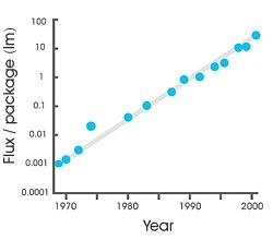
Courtesy of Kessil Newsletter

The High-Brightness LED industry is currently working with SEMI to define needed standards through the HBLED Task Force. The adoption of GEM has been accepted and further investigation is taking place concerning the GEM300 and EDA (Equipment Data Acquisition) standards.

brian-2021website-1

Meet the Semiconductor Standards Expert

Brian Rubow, Director of Solutions Engineering

  • Vice-Chair of SEMI NA RSC (Regional Standards Committee) Organization
  • Co-Chair of SEMI NA Information and Control Global Technical Committee
  • Leader of SEMI DDA and GEM300 Task Forces
  • Leader of SEMI HB-LED Equipment Communications Interface Task Force

Schedule a Meeting