 …never mind which came first… do you know where the chicken and the egg came from?
As integrated circuits increasingly find their way into applications for which human and environmental safety are paramount, the regulatory requirements related to product traceability become ever more stringent. For example, the automotive industry already requires that a device maker be able to provide a full manufacturing process history within 48 hours of a request for certain kinds of products, but this only scratches the surface of what’s to come in the growing markets for autonomous vehicles and their supporting public infrastructure, aircraft components, medical implants and diagnostic systems, and the like.
 The good news in all this is that the latest semiconductor manufacturing equipment interface standards include enough information about the product being built and the processes used at each step along the way to directly support these traceability requirements with little or no custom software. Specifically, the SEMI Equipment Data Acquisition (EDA) suite of standards (also known as “Interface A”) defines the components of an explicit equipment model that can represent this information, and the SEMI E164 (EDA Common Metadata) standard goes so far as to specify the actual structure and naming conventions for the required components.
Before getting deeper into the specifics, let’s step back and define “traceability” in this context. According to ISO 9000 (Quality management systems – Fundamentals and vocabulary), the term means “the ability to trace the history, application or location of an entity by means of recorded identifications.”
In a wafer fabrication facility, this definition covers a broad range of capabilities. The most basic interpretation could be satisfied by simply having an ordered list of the manufacturing equipment visited by each wafer (substrate) during its 3-month journey through the fab. As long as the manufacturer keeps a record of which substrate each assembled die came from (which most do), the required documentation could be generated from information contained in the MES (Manufacturing Execution System) and its associated scheduling/dispatching system.

However, at the other end of the spectrum, the traceability requirement may include not only the list of equipment visited, but also the recipe used at each equipment, the precise timing of wafer movement and process modules visited within the equipment, values of any adjustable recipe parameters and/or equipment constants that affect process behavior, batch identification and status information for any consumables used during the process, usage counts for any fixtures involved, operator interactions (if any), and so on. The reason for this level of detail is to enable the failure analysis engineers to identify the potential root causes for any field failures, and then determine what other devices in the field may be susceptible to similar failure conditions for product recall purposes.
To be sure, much of this information could be assembled after-the-fact from the various data bases maintained by the equipment and process engineering and yield management systems present in most modern wafer fabs, but this process can be complex, time-consuming, and error-prone. A better approach would be to generate the most commonly needed traceability records on-the-fly directly from information available in the equipment... and this is where the newest EDA standards enter the picture.
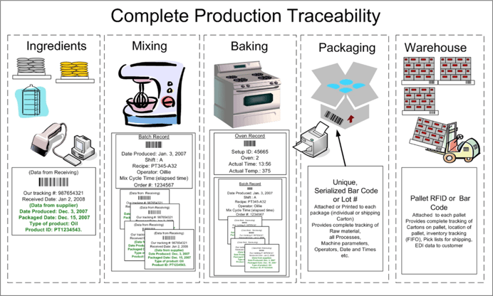
By analogy, let’s look at an intuitive example: a commercial cake baking enterprise. Even for a relatively simple (compared to semiconductor manufacturing) production process, full traceability requires information from the raw materials suppliers through the manufacturing process to packaging and finished goods warehousing. You can see in the picture below that material, recipe, and equipment setup information is included in the records produced.
In a unit of semiconductor manufacturing equipment with an E164-compliant interface, these types of information appear in various sections of the equipment metadata model. Specifically, material-related information is captured in the “Material Manager” logical component, shown in expanded view below* to highlight the state transition events and parameter data available for each substrate during its transportation and processing in the equipment.
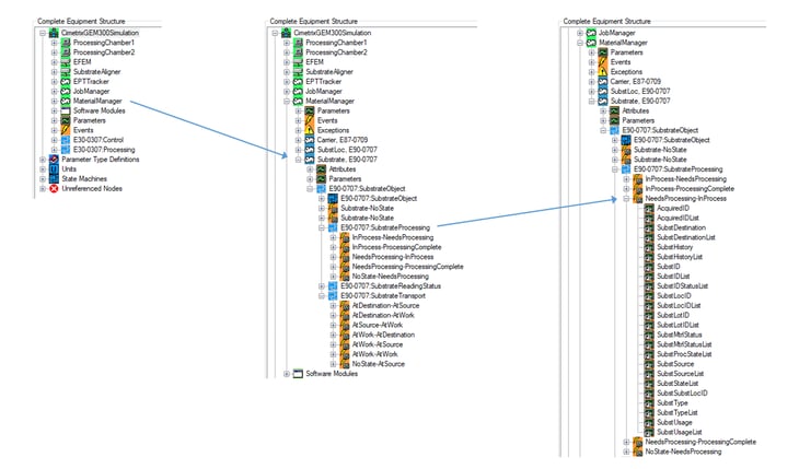
Recipe-related information is found in the physical modules responsible for substrate processing (“ProcessingChamber1” and “ProcessingChamber2” in the example below), within the “E157-0710:ModuleProcess” state machine, dictated by the SEMI E157 (Module Process Tracking) standard and required by E164. Note the rich list of context information available at every recipe step, including the RecipeParameters array, in the expanded model excerpt below.  Taken together, the timing and parameter data from these two sections of the equipment model supply most of the information required for full wafer fab traceability. Moreover, since SEMI E164 actually standardizes the event and parameter names in the model, the DCPs (data collection plans) that collect this information can be programmatically generated and activated for all the equipment that is E164-compliant. This represents a significant engineering cost reduction over the conventional methods used to identify, collect, and manage this information. The figure below is one visualization of such a DCP.
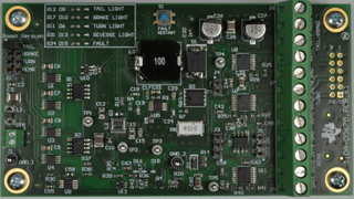
When extended beyond individual devices to circuit boards, modules, and completed parts (see the example below for an automobile speedometer), these requirements require even more bookkeeping… but that’s a topic for another day!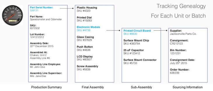
This article is the fourth in the series recently announced in the Models in Smart Manufacturing Series - Introduction, be sure to watch for subsequent postings that will expand on this theme.
We look forward to your feedback and to sharing the Smart Manufacturing journey with you.
*The visualizations of equipment metadata model fragments and DCP contents are those produced by the Cimetrix ECCE Plus product (EDA Client Connection Emulator).