Industry News, Trends and Technology, and Standards Updates

Alan Weber: Vice President, New Product Innovations

Alan Weber is currently the Vice President, New Product Innovations for Cimetrix Incorporated. Previously he served on the Board of Directors for eight years before joining the company as a full-time employee in 2011. Alan has been a part of the semiconductor and manufacturing automation industries for over 40 years. He holds bachelor’s and master’s degrees in Electrical Engineering from Rice University.
Find me on:

Recent Posts

Equipment Data-Driven Continuous Improvement for 200mm Fabs

Posted by Alan Weber: Vice President, New Product Innovations on Feb 23, 2016 1:03:00 PM

Systema1.png

The focus of the most recent SYSTEMA Expert Day, held during a snowy week in Dresden in late January 2016 in conjunction with the 13th annual innovationsforum, was “200mm Fab Enhancement” and featured a number of presentations from Systema GmbH customers and partner companies.

By way of background, there are a number of reasons for the emphasis on 200mm fab enhancement, most notably that many of these factories are enjoying a renaissance of business to meet the growing demands for IoT (Internet of Things) devices. Moreover, since the drivers for this market segment include cost, variety, and volume, the automation and operations people in these factories are faced with a new combination of challenges not seen in earlier markets.

Cimetrix’ contribution to the event was a presentation titled “Equipment Data-Driven Continuous Improvement for 200mm Fabs,” which outlined a model-based, ROI-driven approach for adding equipment data collection capabilities to existing factories. Our basic premise is that such an approach helps meet some of the automation challenges in an incremental, cost-effective way without requiring major redesign of the factory or equipment control systems.

Systema2.png

Since the term “model” is used in many different contexts, we first clarified what this term means in the context of SEMI equipment communications standards, and how this evolved over the past three decades. This was accomplished using a natural language analogy, which is shown in the figure below. Note that the culmination of this process to date is the EDA (Equipment Data Acquisition) metadata model called for in the latest generation of standards, which is very prescriptive in terms of structure, content, and naming conventions for the elements of a semiconductor manufacturing equipment. And even thought the specifics of this model were designed with 300mm wafer fab equipment in mind, the principles well apply to all substrate sizes, and even to the types of material, processes, and equipment found in back end assembly and test factories.

After establishing the value of explicit models for representing equipment, sensors, and other key items in a manufacturing environment, we next introduced concept of an ROI-driven strategy for evaluating the relative benefit of various data collection projects. This strategy first identifies and ranks the key manufacturing objectives that must be addressed, then poses the questions that must be answered to meet those objectives. It then identifies the data sources for the information required to answer those questions, and the data collection techniques (including software) applicable to those sources. Finally, since the original objectives can change with time and additional knowledge, they should be re-examined periodically, giving the strategy an iterative aspect as well.

In order provide specific examples for the uses of equipment data in a continuous improvement program, the presentation listed a number of application use cases that have been successfully deployed in 200mm facilities. These included (in general increasing order of complexity) substrate tracking, process execution tracking, product time measurement (aka wait time waste analysis), external sensor integration, component fingerprinting, and product traceability.

Systema3.png

A couple of these were then explained in more detail, showing how a basic tracking application could start by using a small subset of the equipment data, and then evolve over time to provide more advanced functions (and benefit!) as more detailed information was made available.

For those who want to understand this process in more depth, you are welcome to download the entire presentation using the link below, or call us to discuss how we can apply these ideas to your company!


“Equipment Data-Driven Continuous Improvement for 200mm Fabs"

Watch the Video

Topics: Semiconductor Industry, EDA/Interface A, Data Collection/Management

Manufacturing Applications for Leveraging a Factory-wide EDA Implementation

Posted by Alan Weber: Vice President, New Product Innovations on Dec 16, 2015 8:52:49 PM

In our November EDA-related blog, I covered highlights of the Factory System Infrastructure topic shown in the figure below, and emphasized the need to have a long-term architectural vision to guide the development of a scalable data collection and management environment. Today’s topic completes the picture by summarizing the kind of Manufacturing Applications that can leverage a factory-wide EDA implementation. Unlike infrastructure software alone, these applications are what really provide the ROI for the process engineers and other factory customers of the manufacturing IT department’s efforts, so it is important to understand the scope and requirements of these key applications early in the strategic planning process.

Automation_Strategy_Framework_Mfg_Apps.jpg

Even though Cimetrix is principally in the business of providing software products that enable equipment suppliers to provide data using EDA technology to the factory application developers that use the information in their production systems, we’ve been involved in this process for many years, and have a good idea of the dominant uses of this data to improve manufacturing Key Performance Indicators (KPIs). So in this blog, I’ll cover a little of the high-level picture of what applications fully leverage EDA data.

First and foremost, it is very easy to connect a basic EDA client to a piece of equipment, upload its metadata, and collect information about that tool’s behavior, so implementing a generic “quick-connect production monitor” independent from the fab-wide data collection system is a very common use for EDA. Moreover, if the model in the tool is compliant to the E164 (EDA Common Metadata) standard, you can make a lot of assumptions about the names of the modules, the wafers, the substrate locations, the process jobs, etc., since all of this information is standardized. As a result, you can quickly get an idea of what the equipment is doing, what recipes it is running, what wafers are being processed, and how well the tool is performing with no custom software whatsoever.

Once this is accomplished, the next step most process and equipment engineers take is to more fully characterize the tool’s behavior, so a very common use of EDA is simply improving equipment and process visibility. By inspecting the equipment model, you can see all the events and parameters that are available to be collected, plot them in Excel or on real-time strip charts, or pass them to other analysis applications.

After the equipment has been characterized, the first major production application most fabs will implement is multivariate fault detection (MVA FDC). This is actually the predominant application of EDA data in the industry to date, because in order to do well-architected fault detection applications, one must “frame” the trace data very carefully. High-speed data collection is usually only required in a small number of specific recipe steps after certain conditions have been established, so you can use EDA’s powerful event-based trace data collection to frame the precise data you want, and pass that on to the multivariate control and fault models.

Of course, once you understand a tool’s behavior and have good fault detection capability, you then start to use EDA data to compare tools across a fleet. You would normally want a set of similar equipment to behave in the same way, but perhaps you have one tool that performs exceptionally well, and you’re not quite sure why…In this case, you do what’s called a “golden run” analysis on that equipment, and compare the key trace variables in one with like variables in similar equipment to see where the differences are, and try to explain why those differences exist. Other names for this class of applications include chamber matching and tool matching.

Another key application that we’re starting to see significant interest in is external sensor integration. Factories are now starting to use EDA to present information collected from independent sensors alongside the information collected directly from the equipment. Sharing a common equipment model across these systems effectively “unifies” that data, so the downstream analysis applications believe the information was collected from a single, integrated source. The EDA metadata model offers an ideal way to accomplish this unification.  

Finally, in many advanced wafer fabs, it is important that substrates do not “sit around” after they’ve been processed. Minimizing inter-process wait times is especially important for some advanced processes, so knowing a priori—the precise moment that a lot is going to complete—is a critical capability so the material handling systems can be scheduled to pick up that material and take it to the next process. EDA provides an ideal way to make these predictions generically for multiple process types using the information that is required in the equipment model.

We’ll address these last two applications—external sensor integration and lot completion estimation—in more detail in later blog postings, but I wanted to get you thinking about these ideas early in the discussion of real EDA usage in semiconductor factories.

There are many more EDA application ideas and examples we could share at this point, from component fingerprinting to wait-time waste analysis to dynamic sampling for wafer-level feedback control to feature extraction for predictive maintenance…but these just scratch the surface of what factory customers will come up with once they experience firsthand the flexibility and power of EDA in their factories. More later as this creative process unfolds!

To schedule a time to discuss your EDA needs, click here to set-up a time to talk with one of our knowledgable experts.

Topics: Industry Highlights, EDA/Interface A, Doing Business with Cimetrix

Factory System Infrastructure Support Necessary for a Full-scale EDA Deployment

Posted by Alan Weber: Vice President, New Product Innovations on Nov 24, 2015 12:30:00 PM

In my October 27th blog, I wrote about the Equipment Automation topic shown in the figure below and stressed the importance of developing good equipment purchasing specifications from the outset to ensure the company’s manufacturing objectives can be met. Given the number of EDA pilot and production projects currently active across the industry, it’s likewise important to consider what kind of Factory System Infrastructure will be necessary to support a full-scale EDA deployment… so the purpose of this posting is to highlight this topic for the semiconductor manufacturing IT professionals who may face these challenges soon.

Automation strategy frameworkHowever, before diving into a detailed design process for an EDA factory system, you must decide what overall system architecture will govern that design. A number of factors go into this decision, including 1) the functional requirements that distinguish EDA-based data collection from other more traditional approaches, 2) technology constraints of the existing factory systems, 3) budget limitations, 4) schedule requirements, and especially 5) the non-functional requirements (scalability, performance, reliability, ease-of-use, etc.) that often make the difference between success and failure of a given system.

Each of these factors deserves a thorough treatment of its own, but since we were invited to address this topic at a recent seminar sponsored by SEMI Taiwan, we’ve assembled an overview presentation entitled “Factory Systems Architectures for EDA” that you can use as a starting point. It not only covers in more depth the requirements above which drive key architectural decisions, but also suggests what some of the major architectural components of a production system would need to be, based on the experience Cimetrix has gained working with the earliest adopters of EDA across the semiconductor device maker and equipment supplier communities. These include provisions for handling the scores of equipment metadata models that will exist in a production facility, for creating and managing the thousands of data collection plans that are resident at the equipment instances themselves, for monitoring and maintaining the overall performance of a system with such inherent flexibility, and for a number of other examples. Finally, the presentation describes some high-level examples of architectural “styles” that have been implemented in the industry thus far.  

We sincerely hope you will download this presentation and its companion “The Power of E164: EDA Common Metadata” that was also presented at the SEMI Taiwan event, and contact us when you want to know more about any of these topics.

Topics: Industry Highlights, EDA/Interface A, Doing Business with Cimetrix, Data Collection/Management

Creating Good EDA Purchasing Specifications

Posted by Alan Weber: Vice President, New Product Innovations on Oct 27, 2015 1:00:00 PM

The past few months have been full of news regarding adoption of the SEMI EDA (Equipment Data Acquisition, or Interface A) suite of standards by a number of major semiconductor manufacturers, which has quickly rippled throughout the supplier community as equipment makers and software providers alike consider the implications for their product road maps and support teams.

The range of EDA-related projects now underway covers the full spectrum from basic experimentation with this new data collection paradigm on a couple of tools to integration of these data sources with factory-level predictive analytics platforms to full factory pilot deployments. And although the specific requirements for the equipment suppliers involved in these projects may seem to be very different at the outset, eventually the fab purchasing departments will set a target for EDA interface functionality and performance that is high enough to support their automation requirements for the next 5-7 years.

What this means in practice is that even though the current specifications may be fairly loose regarding which “Freeze” level (I or II) is called for and what the equipment metadata model structure and content should be, eventually the factory customers will fully understand the benefits they can achieve by requiring the latest versions of the entire EDA suite (especially the E164 Common Equipment Metadata standard), and will revise their specifications accordingly. For this reason, it makes perfect sense for equipment suppliers to plan for this level of implementation now rather than waiting for it to be required across the board. This is especially true for suppliers who are just beginning their EDA implementations, as it is no more difficult to build a Freeze II-/E164-compliant interface using today’s EDA development software products than a less capable interface.

From the factory customer usage perspective, it is important to consider the distinguishing features of the EDA standards when developing new purchasing specifications. In particular, unlike SECS/GEM, much of the EDA interface capability is dictated by the structure and content of the equipment metadata model, so this must be carefully designed to ensure that the automation requirements and performance expectations are clearly communicated. This may in turn require more direct involvement of the process, equipment, and industrial engineering teams than ever before.

Automation Strategy frameworkMoreover, when communicating these requirements to the OEM community, it is useful to explain what strategic manufacturing objectives are being addressed and what the information will be used for; this context helps the suppliers understand why the specs may include a high level of detailed information, and can shift a potentially adversarial negotiation process more towards a teaming relationship based on shared objectives.

Fortunately, Cimetrix has many years of experience not only working in the EDA standards development process, but also providing products and services to the early fab adopters of this technology and most of their equipment suppliers. As a result, we have developed a pro forma set of EDA implementation guidelines which can easily be adapted to a specific factory’s purchasing requirements, and are happy to work with you to evaluate your needs and apply this process.  

For more information about developing good EDA purchasing specifications, check out the video we’ve prepared at the link below – and then let us how we can help!

Watch the Creating Good EDA   Purchasing Specifications Video

Topics: Semiconductor Industry, EDA/Interface A

2015 Advanced Process Control (APC) Conference Focused on High Quality Equipment Data

Posted by Alan Weber: Vice President, New Product Innovations on Oct 23, 2015 1:00:00 PM

01_Flags_above_Austin.jpg

02_APC_Conference_Banner.jpg

03_Jalepenos.jpg

04_APC_Conference_Agenda_Cover.jpg

Cimetrix participated in the recent Advanced Process Control (APC) Conference in Austin, Texas, along with more than 120 control professionals across the semiconductor manufacturing industry. This conference, now in its 27th year, is one of only a few global events dedicated to the domain of semiconductor process control and directly supporting technologies, so it was encouraging to see its attendance and energy level rebound from its low water mark a few years ago. The calendar may have indicated it was fall, but nobody told the weather forecasters… Austin set temperature records that week, even hitting 99°F one day!

Given the importance of high quality equipment data for all types of equipment- and factory-level process control applications, it is vital that Cimetrix and its customers understand the current requirements and future direction of this industry segment. Many presentations addressed these topics indirectly, but perhaps the newest insights in this regard came not from the wafer fabrication processes, but rather from the Back End, OSAT (Outsourced Assembly and Test), and advanced packaging segments.

As evidence, a number of presenters mentioned the growing need for equipment data collection in these areas, and cited the following reasons: 1) increasing demands by the consumer product manufacturing customers of these facilities (especially smart phone providers, but others as well) for equipment data to support their product quality and supply chain optimization initiatives; 2) emphasis on the Overall Equipment Effectiveness (OEE) productivity metrics, and the event/status data needed to support their automated calculation; 3) broader deployment of multi-variate Fault Detection and Classification (FDC) applications, which require more equipment trace data parameters than have typically been collected from back end equipment; and finally, 4) actual feedback control based on back end metrology – the best example of this presented last week was an application on dicing equipment that showed how kerf data collection and analysis can be used to adjust saw process parameters

The takeaway for Cimetrix in all this is that the back end equipment suppliers will need to anticipate this demand and may need to upgrade their interface capabilities substantially.

Since some of Cimetrix’ customers have pioneered the application of the latest generation of SEMI EDA (Equipment Data Acquisition) / Interface A standards in plumbing data from external “add-on” sensors to fault detection applications, I presented a generalization of this approach during one of technical sessions. This presentation, “Data Fusion at the Source: Standards and Technologies for Seamless Sensor Integration” is available on the Cimetrix website for those who want to learn more about how this is done.

05_Weber_Presentation_Cover.jpg       Download Presentation  

Check back next week to learn more about creating good EDA/Interface A purchasing specifications.

Topics: EDA/Interface A, Events, Data Collection/Management

EDA Standards Seeing Increasing Adoption Across the Industry

Posted by Alan Weber: Vice President, New Product Innovations on Sep 22, 2015 9:19:21 PM

As mentioned briefly in a previous posting, the adoption momentum for the SEMI EDA (Equipment Data Acquisition) suite of standards has picked up noticeably over the past 6 months, and a number of pilot projects are now underway at leading chip makers across the industry, especially in Asia. As these projects bear fruit, we expect to see explicit requirements for EDA interface capability in the purchase specifications of many more fabs in the coming months. But that’s just a start.

The early adopters of these standards who have now accumulated years of production experience clearly understand that the key to realizing the full manufacturing benefit of this technology lies in the structure and content of the equipment metadata models, which to date have been largely determined by the equipment suppliers themselves. The resulting diversity of EDA implementations is reminiscent of the situation that existed in the days before GEM, when every chip maker required their own particular “dialect” of SECS-II, and the equipment suppliers had to support a custom interface for each customer… not a pretty picture.

Luckily, the standards community recognized this problem early on, and addressed it via the Specification for EDA Common Metadata (SEMI E164). This standard effectively unifies the equipment models across the fab, regardless of process type or supplier, enabling the factory software developers to create generic manufacturing applications that “plug and play” with the equipment to address the problems that are common to all (status and productivity monitoring, material flow, resource utilization, etc.). 

EDA1.jpg

As a result, the next wave of factory implementations can directly leverage these lessons learned by requiring compliance to “Freeze 2, E164” level of the EDA standards suite, and focus their energies on new application development rather than supplier-specific custom integration software. Given the years of experience Cimetrix has dedicated both to the development of the EDA standards in the SEMI community and in providing product-based implementations on “both ends of the wire” (in other words, equipment and client/host side), we can support customers wherever they are in the implementation life cycle, from building awareness to initial purchase specification development to system architecture and application design to conformance and acceptance testing.

For more information about how we can help align your activities with this accelerating adoption process, please contact us… and stay tuned for more specifics on all the above!

For an introduction to EDA, download the presentation Interface A Overview: Characteristics, Benefits, and Applications.

Topics: Industry Highlights, Semiconductor Industry, EDA/Interface A

2015 SEMICON Taiwan Recap

Posted by Alan Weber: Vice President, New Product Innovations on Sep 8, 2015 9:41:00 AM

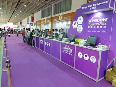
The 2015 SEMICON Taiwan was held at the Taipei Nangang Exhibition Center in the Nangang District of Taipei City, Taiwan September 2-4.  The event drew over 30,000 visitors from all over the world for the three-day event with nearly 1,500 exhibits from a diverse array of companies and organizations across the semiconductor industry.

Blog_pic_2_-_booth.jpg

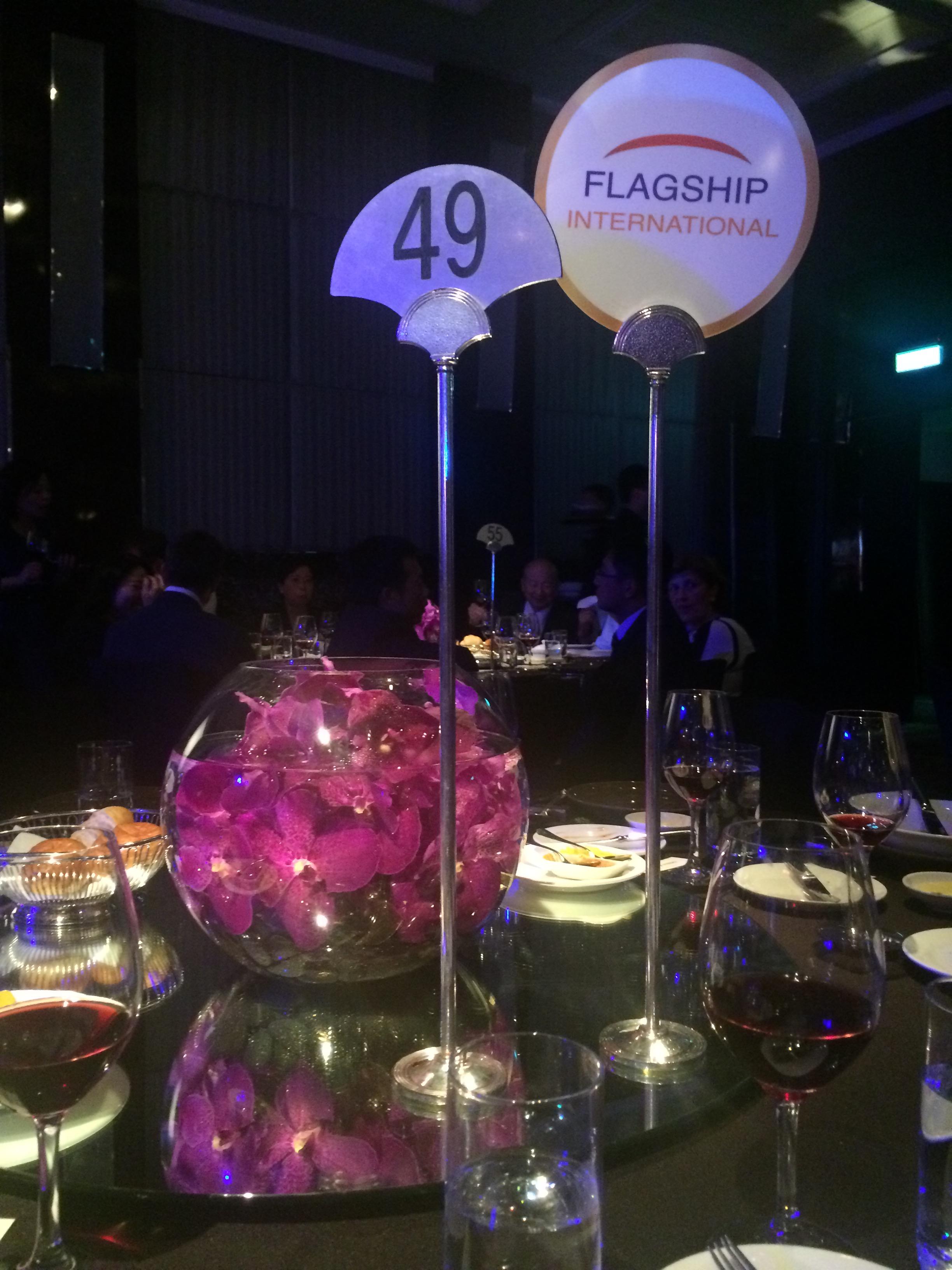
Cimetrix exhibited at SEMICON Taiwan trade show for the first time, in conjunction with its newest Asian partner, Flagship International.

This turned out to be the 20th Anniversary of SEMICON Taiwan, so the mood was especially buoyant and the attendance brisk. SEMI also commemorated the event with a Gala Dinner at the Grand Hyatt on Wednesday night, and we were privileged to attend courtesy of our Flagship colleagues.

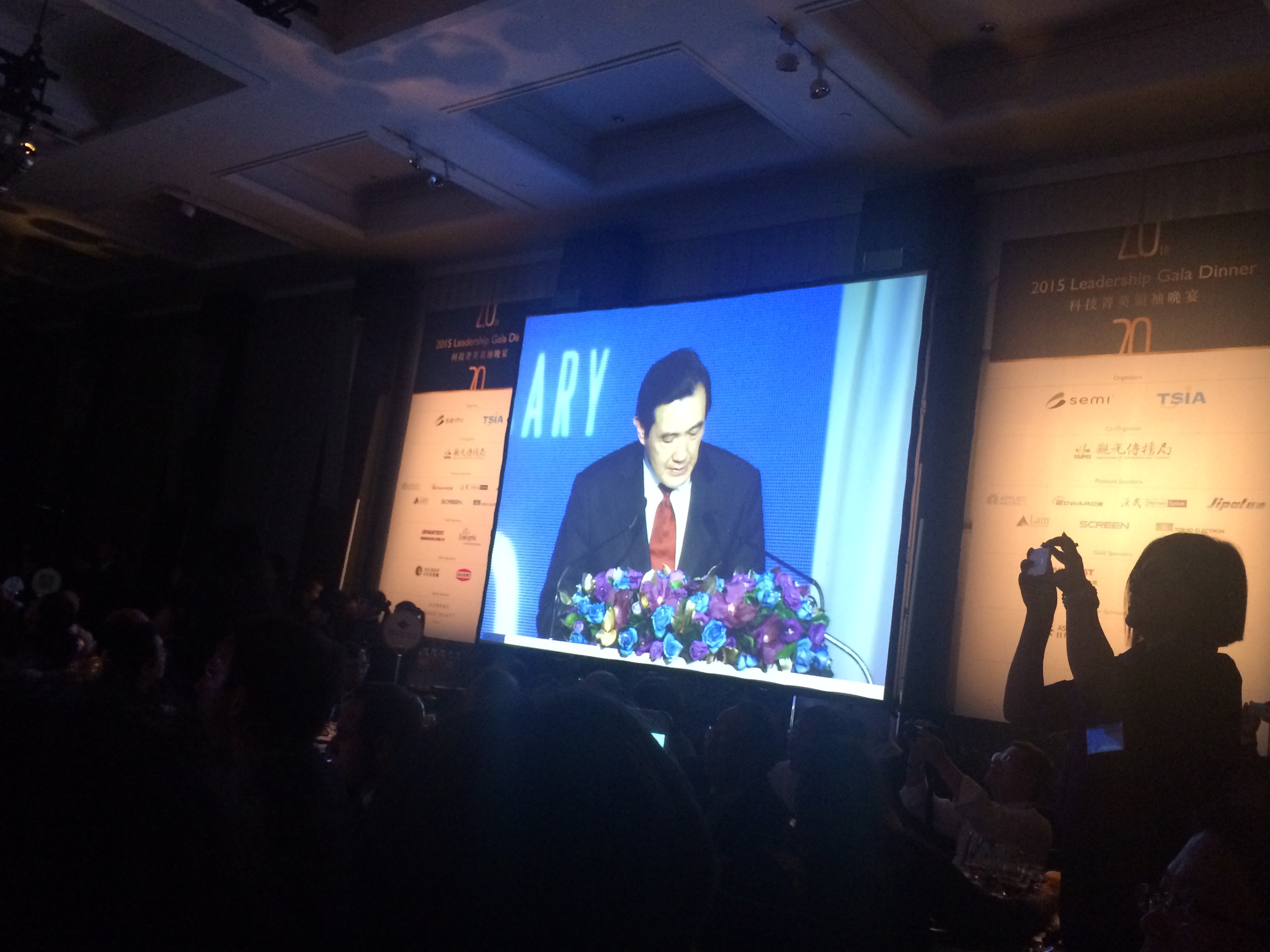
The president of Taiwan, Ma Ying-jeou, even made a guest appearance to thank the semiconductor industry for its contribution to Taiwan’s economic health. 

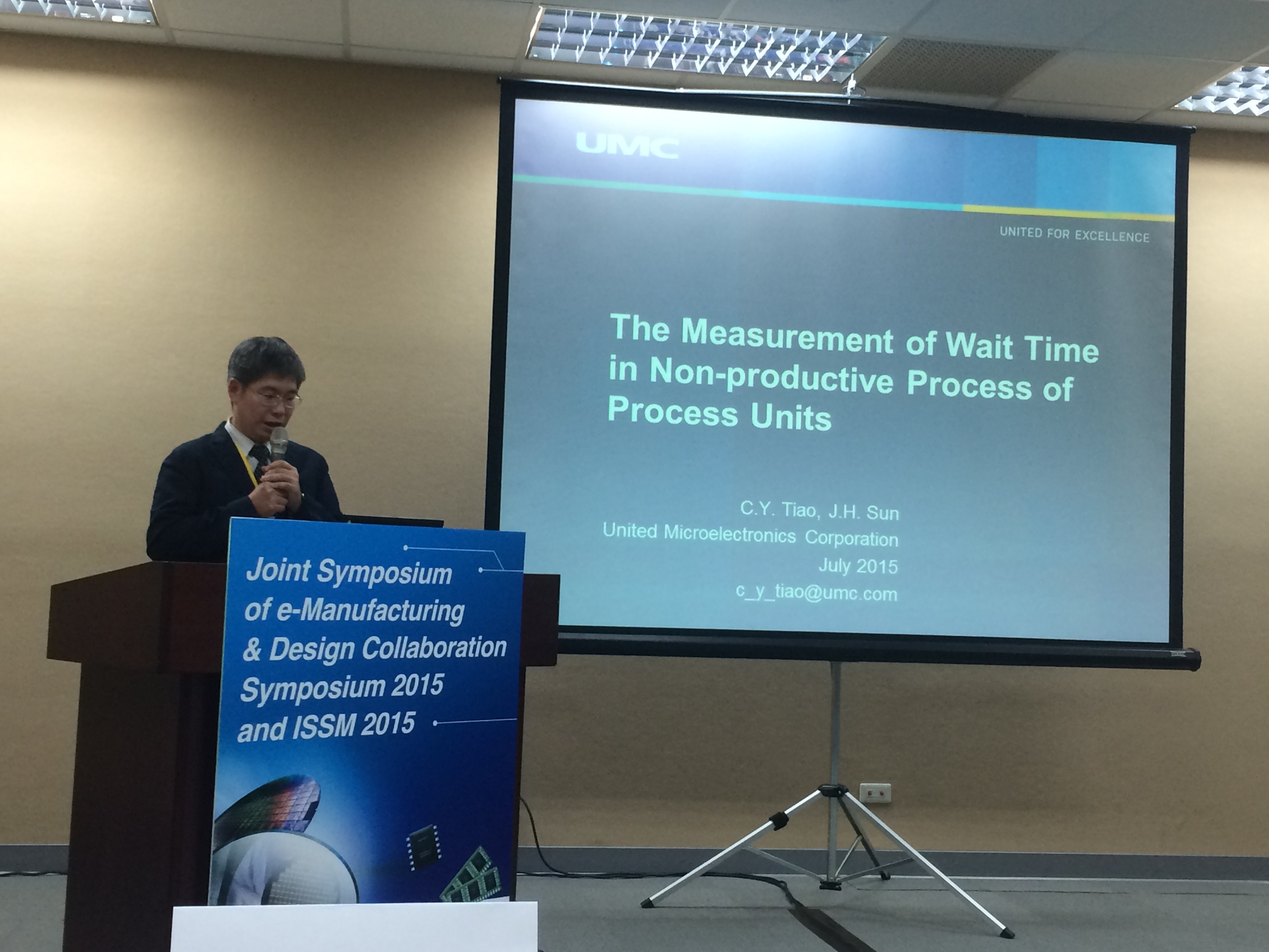
Shortly after the exhibition opened on Wednesday (Sept. 2), a couple of visitors from UMC showed up, and shared the latest work they’ve been doing with the Wait Time Waste (WTW) concepts that we had presented two years earlier. C.Y. Tiao and James Lin of UMC even made two presentations at the eMDC conference on this topic. 

From a standards perspective, this has now taken the form of SEMI E168, Specification for Product Time Measurement (PTM), and has been defined at the “time element” and supporting GEM/SECS message level for process equipment, automated material handling systems (AMHS), and material control systems (MCS). With the advent of SEMI E164 (EDA Common Metadata), these concepts are especially easy to implement, because all the events necessary to calculate the full suite of time elements are required by standard… but more on this is a later blog!

Since much of the world’s foundry capacity is in Taiwan, the equipment industry was well represented at the show, which included many of Cimetrix’ current customers as well as a few local prospects. As a result, Dave Faulkner and Kerry Iwamoto had a chance to visit a number of these firsthand.

Another highlight of the week for Cimetrix was participation in the eMDC (e-Manufacturing & Design Collaboration Symposium), where I made a presentation entitled “Data Fusion at the Source: Standards and Technologies for Seamless Sensor Integration” that addresses the challenges faced by process engineers in effectively using data from an increasing number of sources to analyze process behavior.

The basic idea is to handle the association of necessary context information (lot, substrate, product, layer, process, recipe, step, chamber, etc.) with the raw collected data as close to the source as possible, using a single, integrated model of the equipment and all related data sources. The equipment model that forms the foundation of the EDA/Interface A standards serves this purpose perfectly.


On a final related note, in visiting and talking with a number of the leading chip makers during the week, it seems that the adoption momentum for EDA is now building steadily, so we look forward to supporting this initiative across the value chain. Stay tuned for a late September post that will shed more light on this process!

Topics: SECS/GEM, Semiconductor Industry, Events

History of Semi Equipment Health Monitoring - Fingerprinting

Posted by Alan Weber: Vice President, New Product Innovations on May 31, 2013 3:12:00 PM

I had the privilege of speaking at the annual Advanced Process Control and Manufacturing (APCM) Europe conference in April of this year. The conference supports manufacturers, suppliers and scientific community of semiconductor, photovoltaic, LED, flat panel, MEMS, and other related industries. The topics are focused on current challenges and future needs of Advanced Process Control and Manufacturing Effectiveness. The theme of this year’s conference was From Reactive to Predictive - from SPC to Model-Based Process Control.

My presentation was entitled Fingerprinting and FDC: First Cousins in the Equipment Productivity Family. One of the areas I covered in that presentation was how the whole concept of fingerprinting came about.

I’ve written about Equipment Health Monitoring, also known as fingerprinting, previously – see my blog post about Fingerprinting at SEMICON West at SEMICON West Follow Up: ISMI Fingerprinting Project. While the term fingerprinting has only recently been applied to this technology, the use of this type of application goes back a decade to the advent of Equipment Engineering Systems (EES), when the first major implementation of that technology was in the Renesas factory in Naka, Japan.

The basic idea was that semiconductor manufacturers could learn a great deal by collecting detailed trace and event information from the equipment to understand the behavior of low-level mechanisms, with the assumption that if the low-level mechanisms were exhibiting proper behaviors, then the entire machine would be operating within its specifications. This is the fundamental idea behind fingerprinting.

 Fingerprinting History

Back in 2003, when Renesas was implementing their EES program, there were no good standards for collecting low-level, high-speed trace information, and so the Renesas engineers expended a great deal of effort generating custom interfaces to collect trace and event data they could then feed into a common database. However, as they pursued the effort, they showed what kinds of analysis of the collected data could give them insight into the performance of their fab’s equipment.

As this idea gained traction, Shigeru Kobayashi one of the industry thought leaders at Renesas, proposed through the ITRS and SEMATECH to create a program around the idea of using detailed trace information to improve the equipment quality over time. This suggestion triggered the inception of the EEQA (Enhanced Equipment Quality Assurance) program.

The basic idea of the EEQA program, as it was with EES, was to collect low-level trace information about equipment mechanisms. That data could be shared with the equipment suppliers to show them how the equipment was operating in a production situation in order to improve the design and performance of the machines over time.

The EEQA program lasted more than 3 years at ISMI. There were a number of studies regarding the specific information that equipment engineers and fab engineers could use to characterize different equipment mechanisms and components. There were even a couple of prototypes developed to show how that information could be collected, modeled, and visualized and reported. However, the structural problem with the program was that it placed expectations on the OEMs regarding the amount of data that would need to be collected (and the effort involved in enabling this) without clearly showing the benefit to these suppliers. Consequently, the EEQA program lost support and lay fallow for a while.

However, the basic ideas of EEQA were preserved and folded into a subsequent SEMATECH umbrella program called equipment health monitoring (EHM). However, the energy for the program happened when someone attached an intuitive label to this notion of characterizing a component with its raw data. People attached the term “fingerprint” to that basic model, and the idea of grouping these trace values into a fingerprinting model that would have a specific value that manufacturing can track over time made the basic idea easier to understand and support. When EEQA was re-characterized and re-labeled as fingerprinting, the concept, and understanding the benefit that accrues from collecting and analyzing low-level trace data, finally took hold.

There was one other vital step necessary for the program to catch on in people’s minds. Equipment suppliers and fabs realized that to do predictive maintenance, as well as other health monitoring activities, they needed the data that they could collect using fingerprinting. With the basic concept of a fingerprint understood, and the recognition of the real value that collecting and analyzing the data would provide, both the equipment suppliers and the semiconductor manufacturers began to recognize the need for Equipment Health Monitoring, or fingerprinting.

The key component of any successful fingerprinting program is in-depth equipment domain knowledge, whether that comes from the OEM or from extensive use of that equipment at a specific fab. The OEM is the best official source, but the program can be initiated by the end user as well.

I will discuss more about the presentation at APCM Europe in my next blog post. Stay tuned.

Topics: Semiconductor Industry

Follow Up: Wait Time Waste Project and SEMICON West

Posted by Alan Weber: Vice President, New Product Innovations on Sep 21, 2012 1:57:00 PM

By Alan Weber
Director of Value-Added Products, Cimetrix Inc.

One of the subjects that was of great interest during our very successful SEMICON West 2012 experience was the Wait Time Waste project in which Cimetrix and ISMI/SEMATECH are collaborating. The interest in this project was widespread, and the reason is that, even though both OEMs and semiconductor fabs have focused on improving productivity for decades, they recognize they can still make significant progress with better and more actionable data.

What also intrigues the industry is how to overcome the challenges of gathering and employing the data. For example, there is no standard format for communication logs and equipment logs, and so both OEMs and fabs are discussing the possibility of s a common approach that will work for them. Moreover, the events that may be important to time waste analysis may not be consistently available from the equipment, and now both OEMs and fabs want to know how best to address this issue. Moreover, they want to understand how best to visualize the wafer processing time to determine where to focus their attention.

WTWRI resized 600

These issues, and many more, are discussed in the article I co-authored, “Wait Time Waste (WTW) Metrics, Methodology, and Support Tools”. This article first appeared in Future Fab International, Issue 42,  (c) 2012, www.future-fab.com/, published by Mazik Media, Mill Valley, CA. It not only discusses the background on the subject and the challenges the industry faces, but also discusses future directions for continual enhancement of the time waste analysis.

If you are interested in reading the article, visit: WTW Article.  Contact me at if you have comments or questions at alan.weber@cimetrix.com.

Topics: Events