Industry News, Trends and Technology, and Standards Updates

David Francis: Director of Product Management

David Francis has worked in the semiconductor industry for more than 26 years providing software and services in manufacturing automation. He has experience providing control software for automated material handling systems, scheduling and dispatching systems, SECS/GEM and EDA communications, and equipment control. Francis has lead teams to effectively use software development practices such as CMM/SEI and Agile.
Find me on:

Recent Posts

Software Versioning Help Sets Users' Expectations

Posted by David Francis: Director of Product Management on Jan 14, 2016 1:02:00 PM

There are times in life when a surprise is a good thing. Like when you get a box of chocolates. We all remember the line from the movie Forrest Gump, “Life is like a box of chocolates, you never know what you’re gonna get.” When you install a new version of software however, surprises aren’t as enjoyable. With a new software release, customers need to be able to assess the effort and impact the new release will have on their current systems and procedures. Then they can evaluate whether the new features and functionality will be worth the effort to deploy the new software release. One way software companies can help communicate the impact a new software release may have on customers is by using a clearly defined release versioning procedure.

Change is good and software products that grow and mature over time, adding new features and eliminating unwanted behaviors, can remain healthy and viable over a long period of time. However, consistency and predictability are also important characteristics of good software products. So how do software companies balance these two seemingly competitive objectives?

Itunes.pngsemantic-versioning.pngMany software companies can do this is through the way they use software versioning. It is common for software companies to use a major.minor.patch.build software versioning scheme, for example iTunes 12.3.1. This type of software versioning allows the software company to communicate the scale and impact of the changes in the release to their customers. A change in the “major” release number indicates to customers that there are some significant changes in this release that may impact the way it interacts with the product. The customer will likely need to make code changes or procedural changes when upgrading to such a release. A change to the “minor” release number denotes that there are multiple changes in the release, but customers should see only minor, or possibly no changes, in the way they use the product. A minor release may include some small new features that could potentially require code changes if the customers wants/needs those new features. A “patch” release is generally used to address a specific issue and should not change the customer experience with the software. The build number is most often provided to help the software company when researching a question or customer reported defect.

Software versioning provides a way to set expectations with the customer about what is in the release and how it might affect the way they use the product. It can help take the surprise out of the process of installing a new software release. Life may be “like a box of chocolates,” but software releases shouldn’t be.

If you would like to learn more about the semiconductor industry, software best practices, and other topics related to new technologies, please subscribe to our email updates using the form in the upper right corner of this page.

Topics: Semiconductor Industry, EDA/Interface A, Doing Business with Cimetrix, Cimetrix Products

SEMI Standard E164 Officially Approved

Posted by David Francis: Director of Product Management on Aug 10, 2012 3:52:00 PM

By David Francis
Product Manager

A couple of weeks ago I wrote about our SEMICON West experience and how we expected Ballot 5002B to soon be approved by SEMI as the E164 – EDA Common Metadata standard (see SEMICON West - Ballot 5002B Passes). E164 is now approved, and is available for download on SEMIViews at SEMI E164-0712 - Specification for EDA Common Metadata.

SEMI Logo

The purpose of the E164 specification is to encourage and promote those companies using EDA/Interface A connections to use a more common representation of equipment metadata that is based upon the SEMI E125 Specification for Equipment Self-Description. This will help establish more consistency from tool to tool and from fab to fab, making it easier for equipment vendors to provide a consistent EDA interface and for fabs to develop EDA clients.

The standard was developed because semiconductor equipment suppliers were developing equipment models that were compliant with the E125 standard, but very different from one equipment to the next. Even similar types of equipment had different models, which produced different metadata sets. That scenario was pretty frustrating for fabs as they tried to determine what data they could gather from each piece of equipment.

With E164 approved, equipment suppliers now have a standard they can use to generate the equipment models and fabs now have a standard they can use to generate their client side applications. GLOBALFOUNDRIES has been actively working to adopt the new E164 standard as part of their EDA acceptance criteria. This requirement will help accelerate the adoption of EDA/Interface A as well as the new E164 standard by OEMs and ultimately by other fabs.

Stay tuned – Cimetrix will have some solutions coming soon to support our customers through these changes. If you want to talk with us now about what we can do for an existing project, visit Contact Cimetrix.

Topics: Industry Highlights, EDA/Interface A

EDA/Interface A and ISMI Common Metadata: Guidelines versus Rules

Posted by David Francis: Director of Product Management on Apr 25, 2012 11:05:00 AM

by David Francis
Product Manager

During SEMICON West last year, ISMI made a presentation about a proposed new standard: EDA Common Metadata. EDA stands for Equipment Data Acquisition and is also known as Interface A. The EDA Common Metadata was being balloted as SEMI Document number 5002. That initial ballot failed and so did the next attempt. However, recently, on the third attempt, document 5002B passed SEMI’s Information & Control Committee voting. While it still needs to pass the SEMI ISC Audits & Review Committee before it becomes an official SEMI standard, the 5002B ballot seems to be gaining support.

The SEMI E30, E40, E87, E90, E94, E116, E148, and E157 all define communication and behavior standards for semiconductor processing and metrology equipment. These standards produce the content of the EDA data. The E120, E125, E128, E132, E134, and E138 standards define how to establish and use web services that use SOAP/XML messages over HTTP or HTTPS to transfer data from the equipment to client applications.

So if all these standards already exist for defining EDA content, why was a Common Metadata necessary?

Although he wasn’t talking about SEMI Standards, I think Captain Barbosa in the movie Pirates of the Caribbean: The Curse of the Black Pearl captured the reason best when he said, “The code is more what you would call guidelines than actual rules.” Within the standards there is a lot of room for interpretation regarding the details of how they are implemented. The EDA Common Metadata establishes more specificity around the guidelines for how the equipment data should be represented. The goal is to improve the quality and consistency of the data provided through the EDA interface so that host-side client applications can make better use of the data.

ISMI Logo

In 2010, ISMI announced a new Freeze Version of the EDA standards known as Freeze Version 2 or the 0710 Freeze Version. This defined the specific version of each of the individual EDA standards that should be used by equipment manufacturers to create an EDA interface. For more about the freeze versions for EDA/Interface A, read the Cimetrix Introduction to SEMI EDA/Interface A Standards.

The new SEMI 5002B document provides a single, agreed, interpretation of the various SEMI standards as represented in a common metadata definition, which will help drive consistency in how the standards are implemented. The consistency that should result from the new Common Metadata will help remove some of the uncertainty that may have prevented many companies from developing host-side client applications that can use the EDA data produced by the equipment.


Topics: Industry Highlights, EDA/Interface A

Using EDA/Interface A SEMI Standards

Posted by David Francis: Director of Product Management on Apr 2, 2012 1:19:00 PM

By David Francis

Product Manager

As companies see the improvements in quality and efficiency resulting from the investment in automation over the last decade, there is a greater focus on gathering and analyzing factory data and turning it into actionable information. The implementation of the Equipment Data Acquisition (EDA)/Interface A standards will now allow the industry to further improve the efficiencies in the automated manufacturing facilities by providing access to large quantities of process data.

SEMI (www.semi.org) released the EDA standards in 2005 in order to support the communication between the factory’s data gathering software applications and the factory equipment.

There was no intention of replacing other standards, such as SECS/GEM or GEM 300, and, in fact, EDA does not provide any features for equipment control or configuration. Instead, the EDA standards focus on gathering more data–—particularly state information, sensor feedback, actuator states, and other raw data– necessary for process, product and equipment analysis.

EDA/Interface A Standards Operations Flow


During 2005, IC makers started requiring integrated EDA solutions from the equipment suppliers. Since then, the demand has continued to increase as IC makers roll out plans to improve yield and equipment utilization. Some of the reasons EDA is gaining in popularity are:

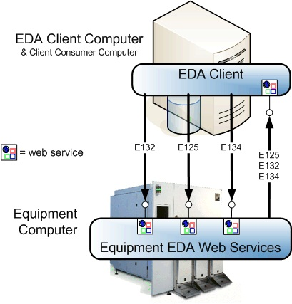
  • EDA supports multiple concurrent clients. SECS/GEM, on the other hand, supports only one client connection, which means semiconductor fabs cannot run several data gathering applications at the same time without an infrastructure to share the data.
  • EDA presents the data in a hierarchy, organized by the major hardware components. By comparison, SECS/GEM data is relatively flat and unorganized, which means that the fab must study the documentation, hardware, software, and processing in order to understand how to organize the data.
  • While data in a SECS/GEM message is highly structured and relatively inflexible, EDA standards use XML, which is inherently designed to accommodate additional metadata
  • SOAP/XML and HTTP are the backbone of most Internet and Intranet applications and there are many programmers worldwide familiar with this technology. On the other hand, only a few industries use SECS/GEM, which limits the worldwide expertise.

Integra ES

There have been developments in EDA/Interface A standards since their introduction. The industry adopted the initial ISMI 1105 freeze version in 2006, and then, four years later, ISMI announced a new 0710 freeze version that includes many improvements and some new capabilities. Cimetrix has learned that equipment suppliers and semiconductor fabs need to discuss and agree upon which freeze version – whether it is 1105 or 0710 – that will be used both for the equipment and the host. In addition, they need to ensure there is a clear understanding of the acceptance testing for the interface.

For more information about the SEMI EDA/Interface A standards, we recommend you request the white paper at Cimetrix Introduction to SEMI EDA/Interface A Standards.

Maybe in a few years we will look back and smile at how common place EDA has become!

Topics: Industry Highlights, EDA/Interface A

A Look Back at 300mm Semiconductor Fabs

Posted by David Francis: Director of Product Management on Mar 26, 2012 10:34:00 AM

By David Francis
Product Manager

I ran across an old issue of Future Fab International – Issue 6 – that I have had since it was published in 1998. I helped write an article that was published in this issue titled “Complete System Integration is Crucial to the Success of 300mm Manufacturing.” The article looked at changes that would be required in semiconductor manufacturing to support the move from 200mm wafers to 300mm wafers.

300mm Wafer resized 600

At the time, I was working for a software company that specialized in the development of Material Control Systems (MCS) for controlling Automated Material Handling Systems (AMHS). Most of the 200mm manufacturing facilities had implemented inter-bay transport systems that move material from one manufacturing bay to another, but within the bays, operators manually loaded wafers onto process or metrology equipment. Operators had to decide what work should be done next, or where the material should go after each process, after reviewing choices from a dispatch screen. There were islands of automation, but not much integration.

With the size, weight, and bulk of the 300mm carriers, transport systems would need to deliver material directly to the processing or metrology tool. This required very tight integration between the MCS, the dispatching system, and the factory Manufacturing Execution System (MES). In 1998 the GEM300 standards that would make all this possible had not been adopted very widely yet and were only starting to get semiconductor equipment suppliers’ attention.

This old article talked about the need for developing a reliable, low-footprint intra-bay transport system. It also explored the new concept of having the dispatch system make the decision about what work to do next rather than just suggesting what could be done. The MCS would need to interface with the dispatching system to be able to position material close to where it would be needed for processing.

The SEMI GEM 300 standards started gaining traction about the year 2000 and the idea of “lights out” manufacturing soon became a reality. It has been exciting to watch as the MES, dispatcher, AMHS and MCS systems have progressed and the fully automated, integrated manufacturing environment described in the article has become a reality.

Semiconductor Fab resized 600

While the move to 450mm wafers is probably still a few years off, I expect that transition will be much easier than the transition from 200mm to 300mm because of the work done for 300mm factories. The standards are well established, the control systems have matured, and the integration of the various components is very stable. It is exciting to see these future visions become common practice.

Recently, Cimetrix updated our Introduction to SEMI GEM 300 Standards white paper.  We have refreshed the content to answer some of the questions many people pose to us. Take a look and let us know what you think.

Topics: Industry Highlights, SECS/GEM, Cimetrix Products, GEM300

Adoption of EDA/Interface A SEMI Standards

Posted by David Francis: Director of Product Management on Mar 16, 2012 9:58:00 AM

By David Francis
Product Manager

This is an exciting time for Cimetrix as we see equipment suppliers and semiconductor fabs adopt the SEMI Equipment Data Acquisition (EDA)/Interface A standards. As equipment suppliers use our CIMPortal™ Plus software development kit, and fabs use our EDAConnect™ and ECCEsoftware, there is a growing awareness of how fabs can use the increased data that they gather to improve productivity and reduce unit costs.

EDA client and equipment resized 600

One thing for certain is that equipment suppliers and semiconductor fabs need to communicate with each other effectively regarding their plans for implementing EDA. This includes determining which EDA Freeze Version they will use, freeze version 1105, freeze version 0710, or perhaps a mixture of both depending on tool type. The fab will also need to specify their equipment acceptance criteria. The acceptance tests need to be comprehensive, but optimized to keep the overall installation cost at a minimum.

To support equipment integration into the fab, the EDA interface can provide descriptions of the equipment's structure and behavior to the factory control systems. These metadata sets include the equipment components, the events and exceptions that can be reported, and all the available data parameters. A predictable and reliable interface definition enables faster equipment integration and lower installation cost.

To help ensure consistent metadata, ISMI is providing a tool to check for conformance of equipment metadata to EDA standards (such as E120 Specification of the Common Equipment Module and the E125Specification for Equipment Self-Description) and EDA guidelines. 

Cimetrix was at the forefront of the EDA/Interface A standards development and continues to be involved with the efforts around the new standards and the creation of the new EDA Client Connection Emulator (ECCE) version 2, which supports both 1105 and 01710 versions of the standards. It is great to see the broader adoption of the standards and the recognition of how the standards can help increase fab productivity.

To read more about SEMI EDA/Interface A standards, visit ourEDA/Interface A web page.

Topics: Industry Highlights, EDA/Interface A

Equipment Data Acquisition (EDA) – The Sequel

Posted by David Francis: Director of Product Management on Sep 8, 2011 11:00:00 AM

By David Francis

Product Manager

ISMI held a very successful EDA/Interface A workshop at SEMICON West in July, and Cimetrix was a guest speaker at the workshop.  The attendance and interest in EDA was surprising, given that EDA has been discussed for five years with very little adoption to-date.  Now, however, we see a major change occurring.

In November 2005, ISMI established the first freeze version of the Equipment Data Acquisition (EDA) Standards to enhance adoption by eliminating the “moving target” issue; it was known as the 1105 Freeze Version. The industry had good reasons for developing EDA. Fabs could get significantly higher trace data collection throughput, and the robust tool model in EDA provided better access to sensors and other key equipment variables useful for operational data monitoring.  Moreover, EDA greatly simplified the creation of data collection plans (DCP), so fab engineers could resolve manufacturing problems faster and easier. Best of all, it decoupled data collection from SECS/GEM, so data collection would not be influenced by tool control nor would tool control performance be impacted by collection of large quantities of data.  The result would be that fabs would benefit from more sophisticated automatic process control (APC) algorithms, improved yields, and reduced downtime.

Unfortunately, only a few brave equipment suppliers started work on developing interfaces for their equipment to comply with the 1105 Freeze Version. Not surprisingly, the general adoption and excitement in the industry around EDA didn’t last long in the absence of strong support from semiconductor manufacturers and foundry customers.

Why? It generally takes a significant amount of time for equipment suppliers and semiconductor manufacturers to review the standards and introduce new systems to deliver and consume the data. In the case of EDA this was further compounded because of bad timing in the industry.  The 1105 freeze version of EDA came out during a boom time for the semiconductor industry, when fabs want to avoid making significant changes that could disrupt production.  By the time the equipment vendors could develop new systems with an EDA interface, the industry experienced the biggest – and fastest – downturn in history.  In 2008-2009, semiconductor companies were buying very few new machines, let alone starting new fabs.

 C  Users rschreck Documents Marketing Blogs Final Blogs Fab Forecast resized 600

But, when business in the industry turned back up in 2010, both GLOBALFOUNDRIES and Toshiba announced they would build new 300mm fabs, and would require OEMs to supply new equipment with an EDA interface.  In addition, there are other semiconductor manufacturers and foundries who are investigating and starting to use EDA, but have not been as vocal about adopting the standard.

 C  Users rschreck Documents Marketing Blogs Final Blogs GF Fab1 resized 600

 GLOBALFOUNDRIES Fab 1 in Dresden, Germany

Also in 2010, ISMI announced the second freeze version (the 0710 Freeze Version) of the EDA Standards. Since that announcement, there has been a lot of interest and activity in the industry surrounding Interface A. One reason, obviously, is that the two large semiconductor manufacturers have added Interface A to their equipment purchase specifications and acceptance criteria, so equipment suppliers want to ensure that their products comply with these new requirements.

But there are other reasons for interest in EDA.  The 0710 freeze version provides a number of simplifications and clarifications of the 1105 freeze version. For example, there is better linkage between the SECS/GEM events and variables and the EDA constructs, and the metadata is simpler. There have also been other changes, like using simple events as an alternative to complete state machines, and allowing DCP behavior to be separate for each client. As the industry tackles 3D designs with ever smaller geometries, the process window gets a lot narrower and access to data and applications to consume this data become imperatives instead of “nice-to-haves.”

In addition, ISMI has updated its EDA Guidance document to more fully describe how to implement EDA interfaces. In parallel, ISMI partnered with Cimetrix to develop the new version of the Equipment Client Connection Emulator (ECCE) that OEMs and semiconductor manufacturers can use to verify EDA interfaces (see New Freeze Version of Interface A Requires New ECCE Version). Finally, the ISMI/NIST Metadata Conformance Analyzer (MCA) is also available to check for conformance of equipment metadata to the applicable portions of the SEMI standards and ISMI guidelines.

It is exciting to see the renewed interest and attention to EDA. Is all the attention because semiconductor manufacturers are starting to require EDA, or are semiconductor manufacturers starting to require it because of all the recent interest? Either way, there are genuine opportunities for both equipment suppliers and semiconductor manufacturers to make use of data collected through EDA to improve efficiencies and open new capabilities for microelectronics manufacturing.

Topics: Industry Highlights, EDA/Interface A

GEM300 - All of This Chaos Makes Perfect Sense

Posted by David Francis: Director of Product Management on Jan 20, 2011 1:23:00 PM

xby David Francis
Product Manager, Connectivity Products

Back in the 1990s, Joe Diffie released an album titled “Third Rock from the Sun.”  I have to admit I liked the title song, especially the chorus:

Cause and effect, chain of events
All of the chaos makes perfect sense
When you're spinning round
Things come undone
Welcome to Earth 3rd rock from the Sun.”

 Joe Diffie resized 600

At the time, I was working with Motorola in Austin developing host-side cell control applications for one of their new fabs.  Motorola had implemented some rudimentary equipment control and data collection in their older fabs, but the standards were loosely defined at that time and the equipment interfaces were inconsistent. We realized we could not replicate the work implemented in the old fabs into the new fabs, yet we did not have solid standards to use for the new fabs.  As the song said, we were “spinning round in this chaos.

What eventually drove more clarification in the GEM/GEM300 standards was the industry-wide push to move to fully automated 300mm IC manufacturing.  The larger wafers offer much greater productivity and throughput, with significantly lower cost per die, and SEMI wanted to ensure the industry had a well-understood and approved interface standard for the equipment used to manufacture semiconductors on these much larger wafers.  Those new standards made it easier and more cost effective to create the host-side cell control applications.  Now the chaos started to “make perfect sense.”

Embracing the GEM/GEM300 standards allowed IC manufacturers to purchase standard software components to analyze manufacturing processes and identify opportunities to increase productivity.  In other words, they wanted to bring order to all the chaos.  The alternative – developing their own data analysis applications for each fab – would have been very expensive and time consuming.  SEMI brought order to the scene by offering the GEM/GEM300 standards that all the equipment vendors and fabs could use.  Now OEMs could develop equipment needed for automated wafer processing with the confidence fabs could install the machines and link them to their networks.  Fabs could increase throughput and drive down cost per die, and, just as important, gather data necessary to increase manufacturing efficiencies even more.

Fast forward twenty years, and we see a very similar situation, this time caused by the impressive growth in Photovoltaic cell and LED manufacturing.  The fabs in those industries need more advanced equipment to increase throughput and drive down unit costs in order to meet demand.  However, up to this date, both sectors are reluctant to adopt the GEM standards.  They are concerned those standards may be too big and complex for their processes, which are simpler than the current state-of-the-art semiconductor fab processes.  Once again, we see the chaos that occurs with explosive growth and companies seeking a solution to bring order to their processes.

Since I’ve seen this story before - and heard the music played time and time again - I know that adopting communication standards will help PV and LED manufacturers continue their drive to reduce unit costs and drive demand.  The effort is underway in the PV sector with the PV2 standard.  The LED sector should also look to adopt existing standards, or do what the PV sector has done and develop their own standards.  Either way, we know that standards help all the “chaos make perfect sense.”

Topics: SECS/GEM, Semiconductor Industry, Photovoltaic/PV Standards