It’s amazing enough to think that a single factory can start 100,000 wafers every month on their cyclical journey through 1500 process steps… and have 99%+ of them emerge 4 months later to be delivered to packaging houses and then on to waiting customers. It’s quite another to realize that all of this happens continuously (24 x 7) and automatically. 
“How is this possible?” you ask.
Well, a big part of the solution is the body of SEMI standards which have evolved since the early 80s to keep pace with the ever-changing demands of the industry. From an automation standpoint, many of these standards deal with the communications between manufacturing equipment and the factory information and control systems that are essential for managing these complex, hyper-competitive global enterprises.
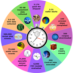
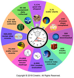
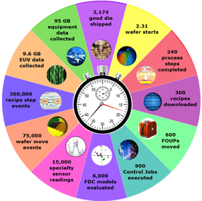
A significant characteristic of these standards is that they have been carefully designed to be “additive.” This means that new generations of SEMI’s communications standards do not supplant or obsolete the previous generations, but rather provide new capabilities in an incremental fashion. To appreciate the importance of this in actual practice, consider how the GEM, GEM300, and EDA/Interface A standards support the transactions that occur in a single Gigafab Minute.
Starting at 1:00 o’clock on the infographic and moving clockwise, you first notice that 2.31 wafers enter the line. Of course, these are actually released in 25-wafer 300mm FOUPs (Front-Opening Unified Pod), but 100K wafers per month translates to 2.31 per minute. Since these factories run continuously, once the line is full, it stays full. And with an average total cycle time of 4 months, this means that there are 400K wafers of WIP (work in process) in the factory at any given time. This number, and the total number of equipment (5000+), drive the rest of the calculations.
GEM (Generic Equipment Model) – SEMI E30, etc.
The GEM messaging standards were initially defined in the early 90s to support the factory scheduling and dispatching applications that decide what lots should go to what equipment, the automated material handling systems that deliver and pick-up material to/from the equipment accordingly, the recipe management systems that ensure each process step is executed properly, and the MES (Manufacturing Execution System) transactions that maintain the fidelity of the factory system’s “digital twin.”
Every minute of every day, GEM messages support and chronicle the following activities: 240 process steps are completed (i.e., 240 25-wafer lots are processed), 300 recipes are downloaded along with a set of run-specific adjustable control parameters, and 600 FOUPs are moved from one place to another (equipment, stockers, under-track storage, etc.). For each of these activities, the factory’s MES is notified instantaneously.
GEM300 – SEMI E40, E87, E90, E94, E157
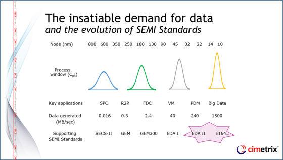
With the advent of 300mm manufacturing in the mid-to-late 90s, a global team of volunteer system engineers from the leading chip makers defined the GEM300 standards to support fully automated manufacturing operations. Starting at 5:00 o’clock on the infographic, the number of transactions per minute jumps almost 3 orders of magnitude, from the monitoring of 900 control jobs across 4000 process tools to the tracking of 360,000 individual recipe step change events. This level of event granularity is essential for the latest generation of FDC (Fault Detection and Classification) applications, because precise data framing is a key prerequisite for minimizing the false alarm rate while still preventing serious process excursions. In this context, more than 6000 recipe-, product- and chamber-specific fault models may be evaluated every minute.
Simultaneously, the applications that monitor instantaneous throughput to prevent “productivity excursions” and identify systemic “wait time waste” situations depend on detailed intra-tool wafer movement events. In a fab with hundreds of multi-chamber, single-wafer processes, 75,000 or more of these events occur every minute. 
EDA (Equipment Data Acquisition) – SEMI E120, E125, E132, E134, E164, etc.
Rounding out the SEMI standards in our example gigafab is the suite of EDA standards which complement the command and control functions of GEM/GEM300 with flexible, high-performance, model-based data collection. The EDA standards enable the on-demand collection of the volume and variety of “big data” required from the equipment to support the advanced analysis, machine learning, and other AI (Artificial Intelligence) applications that are becoming increasingly prevalent in leading semiconductor manufacturers. As EUV (Extreme Ultraviolet) lithography moves from pilot production to high-volume manufacturing at the 7nm process node and beyond, the litho process area will become a major source of process data by itself, generating 10 GB of data every minute. This is in addition to the 100 GB of data collected from other process areas. 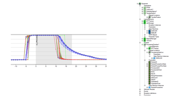
The End Result
The final wedge (12:00 o’clock) in our infographic highlights the real objective – which is producing the millions of integrated circuits that fuel our global economy and provide the technologies that are an integral part of our modern way of life. Assuming a nominal die size of 50 square mm (typical of an 8 GB DRAM), the 2.31 wafers we started at 1:00 o’clock result in almost 3200 individual chips. But none of this would be possible without the pervasive factory automation technology we now take for granted. So, as you finish reading this posting on whatever device you happen to be using, take a micro-moment to acknowledge and thank the hundreds of standards volunteers whose insights and efforts made this a reality!
 You may not be responsible for running a gigafab anytime soon, but the SEMI standards used in this setting are no less applicable to any Smart Manufacturing environment. Give us a call if you’d like to know more about how these technologies can benefit your operations for many years to come.
You can see this infographic and much more in the Cimetrix Resource center.

*The Gigafab Minute was inspired by an analogous explication of the scope and impact of today’s Internet from Lori Lewis and Chadd Callahan of Cumulus Media, and published on the Visual Capitalist web site (http://www.visualcapitalist.com/internet-minute-2018/)


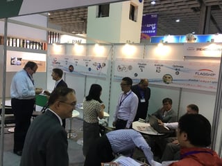
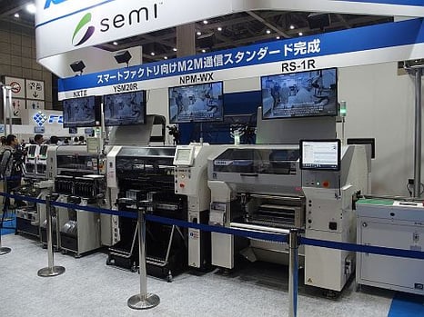
 Cimetrix attended the recent JISSO PROTEC exhibition (June 5-7, 2019) at the Tokyo Big Sight International Exhibition Center to see the latest developments in SMT (Surface Mount Technology) manufacturing… and witnessed a truly compelling demonstration of the new SEMI Flow Manufacturing communications standards in action.
 The new suite of standards is named SMT-ELS (Surface Mount Technology-Equipment Link Standards), and includes SEMI A1/1.1 as a lower-level messaging standard with SEMI A2 SMASH (Surface Mount Assembler Smart Hookup) defining the content of the messages required to configure an SMT manufacturing line and automate the material and information transfer among all equipment in that line. This is depicted in the figure below.
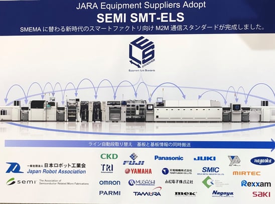


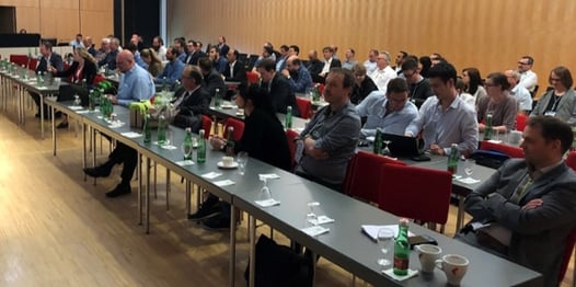
 Cimetrix participated in the recent European Advanced Process Control and Manufacturing (apc|m) Conference, along with over 150 control professionals across the European and global semiconductor manufacturing industry. This site of this year’s conference was Villach, Austria, a picturesque town nestled in the eastern Alps just north of the Italian border in the state of Carinthia. This region is home to a number of high-tech companies and institutions all along the semiconductor manufacturing value chain, and since it was the first time the conference was held in Villach, the local hosts rolled out the red carpet.
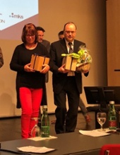
 Other highlights of the conference included:
 Another invited talk from BMW was delivered by Rainer Hohenhoff which covered “Product Data and Product Life Cycle Management in the face of new business models of the automotive industry.” In short, it discussed many of the ways a car company might make money even after people stop buying as many cars as they do today… and what collisions (pun intended) you could expect in the market as service companies like Google, Amazon, UBER, and others converge on the transportation consumer.
  The insights gained from these and the other 30+ presentations are too numerous to list here, but in aggregate, they provided an excellent reminder of how relevant semiconductor technology has become for our comfort, sustenance, safety, and overall quality of life.
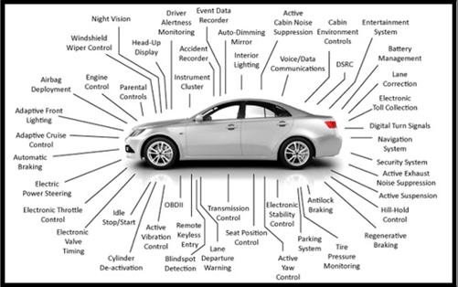
 But the full impact of automotive electronics includes all the infrastructure technologies external to the car, such as 5G telecommunications, “smart” roads and traffic signals, routing and congestion management systems for major cities, satellite systems that provide GPS information, entertainment content providers for the non-drivers, and law enforcement, just to name a few. And as driverless cars approach commercial feasibility, the scope and importance of these systems increase significantly.
 The automation requirements for the most advanced fabs call for the latest versions (Freeze II) of all the standards in the EDA suite, including the EDA Common Metadata (E164) standard. Dealing with older versions of the standard in the factory systems creates unnecessary work and complexity for the fab’s automation staff, so it is best to implement the latest versions from the outset. The Cimetrix CIMPortal Plus product makes this a straightforward process using the model development and configuration tools in its SDK (Software Development Kit), so there is absolutely no cost penalty for providing the latest generation of standards in your interface.
  This is why the most advanced fabs have been far more explicit in their automation purchase specifications with respect to equipment model content, going so far as to specify the level of detailed information they want to collect about process performance, equipment behavior, internal control parameters, setpoints and real-time response of common mechanisms like material handling, vacuum system performance, power generation, consumables usage, and the like. This level of visibility into equipment operation is becoming increasingly important to achieve the required yield and productivity KPIs (Key Performance Indicators) for fab at all technology nodes.
  Before the fab’s automation team can fully integrate a new piece of equipment, it must follow a rigorous acceptance process that includes a comprehensive set of interface tests for standards compliance, performance, and reliability. This process is vital because solid data collection capability is fundamental for rapid process qualification and yield ramp that shorten a new factory’s “time to money.” If you know what acceptance tests and related software tools the fab will use (which is now explicit in the latest EDA purchase specifications), you can purchase the same software tools, perform and document the results of these same tests before shipping the equipment.


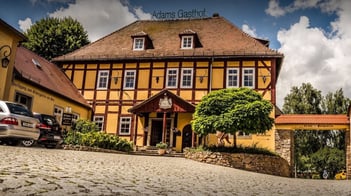
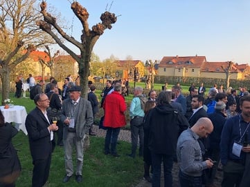
 Cimetrix participated in the recent European Advanced Process Control and Manufacturing (apc|m) Conference, along with over 160 control systems professionals across the European and global semiconductor manufacturing industry. The conference was held in Dresden, a beautiful city in the Saxony state of Germany which was the site of the original European conference in 2000 and host to this annual event many times since.
 “FDC to the power of 2 – how it got us to the next level of manufacturing excellence“ by Jan Räbiger of GLOBALFOUNDRIES – one of a number of long-time thought leaders in the development and application of APC technology, Jan described the latest phase of FDC system evolution, which includes broad use of the EDA/Interface A standards to zero in on recipe step-specific anomalies that had previously escaped detection.
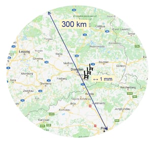


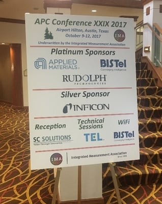
 Austin, Texas was the site of this year’s conference, going back to its roots after almost 30 years. Because of its unique focus on equipment and process control technology for the semiconductor industry, and the consistently high quality of its technical content, this conference continues to attract both industry veterans and newcomers to this domain, with this year’s attendance over 160.