Industry News, Trends and Technology, and Standards Updates

Why choose a commercial product for the EDA (Equipment Data Acquisition) interface solution for your equipment? 为什么要为您的设备选择商用EDA解决方案?

Posted by Clare Liu (刘波); Solutions Engineer on Nov 20, 2018 11:10:00 AM
Lessons-Learned-small

Clare Liu, a Cimetrix Solutions Engineer, goes over the pros and cons of choosing a commercial product for EDA/Interface A vs. building a solution from scratch. Read it now in Chinese, or below in English. 

本文的焦点是当许多半导体设备制造商面对他们那些最先进的客户提出的自动化需求时,如何在购买支持EDA(Interface-A)标准的软件产品,或者自主开发之间做出决策。

鉴于我本人在今年初加入Cimtrix之前,曾经在一家半导体装备公司里担任EDA标准实现项目的主要开发人员,我想解释说明一下选择商业解决方案的利与弊。

1. 经验

在半导体制造设备上实现EDA要求软件开发人员具有半导体行业标准(SEMI)和半导体设备的经验。这对大多数设备供应商来说是非常困难的。即使他们已经拥有良好的软件开发人员,经验丰富的工厂自动化工程师和一个完整的硬件设计团队,他们还是需要有效的共同协作,找出如何设计一个结构良好的设备模型(SEMIE120 CEM 通用设备模型规范)并将设备所有的变量、时间和报警映射到设备模型的各个节点上(SEMI E125 EqSD设备自我描述规范)。 一个商业的EDA解决方案能够同时为OEM提供这些知识,并且可以基于该设备,提供EDA开发过程的指导方针。

2. 验收

checkmark简单地实现EDA接口功能和正确有效地实现的结果是不一样的。我从中得到的教训之一是,我们花了几乎整整一年的时间来实现EDA Freeze I的各种功能,并为测试的需要开发了客户端软件。然而,当我们将我们的EDA解决方案发布给客户工厂时,他们使用权威的第三方测试软件产品对所有设备的EDA解决方案进行了验证。我们的实现最初没有通过验收,因为我们对EDA标准的理解与客户的理解有些差异。为此我们花了很长时间来逐一解决验收中遇到的问题。商业的EDA解决方案通常已经在许多工厂得到了验证,因此更加标准化。

gantt-chart-cimetrix3. 时机

一个商业的EDA解决方案可以帮助OEM在短时间内开发出合格的EDA接口。自主开发EDA会给本已紧张的交付进度增加时间压力,如果需求来自一个新客户,第一个支持EDA标准的设备供应商通常会更有优势。在业务方面,EDA功能很有可能是获得订单的关键。在技术方面,第一个EDA的使用会成为整个Fab的范例,可以被用来制定其他设备在生产环境中必须满足的操作要求。

4.服务

使用商业EDA解决方案通常包括来自软件供应商的良好的技术支持,这些技术支持可能包含在最初的许可证费用中,或者是单独的技术支持合同。这意味着OEM公司不需要维持一个专门的软件团队来维护和解决遇到的软件问题。相反,他们可以依靠更专业的支持团队,而不用担心任何内部开发人员离开公司所带来的影响。

5. 知识更新

由于很多改进得到认同,还有很多新的技术在关键产品中的使用变得可行,半导体行业的EDA标准每年都在发生变化,在写这篇文章的时候,一个新的EDA标准冻结版本Freeze III正在投票中。商业EDA解决方案通常会紧紧追随标准的发展,同时会不断根据其他工厂用户的请求增加新的功能。这使得OEM能够快速、可靠地响应客户的最新需求。

1.成本

OEM必须为商业软件的许可证,以及可能的、每年的技术支持支付费用。

2.知识产权(IP)

一些OEM公司为了对EDA功能的源代码有完全的控制权和所有权,他们选择自主开发并拥有这些软件,其原因是大多数商业软件包通常不会为基本许可证的使用者提供源代码。

3.修复错误的时间

如果在商业软件包中发现错误,设备工程师甚至工厂客户可能需要帮助软件供应商找到根本原因。他们还必须等待供应商修复并发布新版本的软件。这对于使用者来说非常不方便。

如果您的公司正面临这样的决定,请联系我们——我们很乐意分享我们的专业知识和市场知识,并协助您做出明智的决定。

Schedule a Meeting

您可能还对以下信息感兴趣:

View Presentation: Raising the Bar
View Video: Importance of Process Module Tracking
View Video: E164 EDA Common Metadata
View Video: Equipment Modeling - E120/E125
Learn about CIMPortal 


Lessons-Learned-smallThe focus of this blog posting is the decision that many semiconductor manufacturing equipment suppliers face when deciding how to address the automation requirements of their most advanced customers, namely, whether or not to buy a commercial software package that supports the SEMI Equipment Data Acquisition (EDA / Interface A) Standards, or to develop this capability in-house.

I am especially qualified to explain the pros and cons of choosing a commercial solution, having worked as the EDA standards implementation lead developer in an equipment supplier before joining the Cimetrix team earlier this year.

  • Pros

1. Experience

Implementing EDA on a single unit of semiconductor manufacturing equipment requires that the software developers have experience with both SEMI Standards and the equipment. This is very difficult for most equipment suppliers. Even if they have good software developers, experienced factory automation engineers and a complete hardware design team, they must still work together efficiently to figure out how to design a well-structured equipment model (SEMI E120 CEM) and map all the equipment variables, events and alarm to the CEM nodes (SEMI E125 Equipment Self-Description).  A commercial EDA package provides all this knowledge for the OEM and guidelines explaining the EDA development process for their systems.

2. Qualifications

checkmarkSimply being able to implement the EDA interface functions is not the same as implementing them in a robust fashion. One of my lessons learned is that we spent almost an entire year to implement the EDA Freeze I version of the standards and the client software required to test these functions. However, when we released the EDA interface to the factory customer, they qualified the EDA solution for all equipment modules with an authoritative third-party compliance testing software product. Our implementation failed at first because our understanding of the SEMI Standards specifications was different from the customer’s understanding. So we struggled for a long time to fix all the problems.  A commercial EDA package will necessarily have been proven in many sites and is therefore far more standardized.

3. Timing

gantt-chart-cimetrix

A commercial EDA product can help the OEM develop a qualified EDA interface in a short time. Developing EDA in house adds time pressure to already tight delivery schedules, and if the requirements are coming from a new customer, the first equipment supplier supporting EDA standards may have an advantage. On the business side, EDA might be the key feature to get the order. On the technical side, the first usage may determine the approach used across the entire fab, thereby dictating operational requirements that the other equipment must meet in the production environment.

4. Service

Using a commercial EDA package normally includes good technical support from the software supplier; this may be covered in the initial license fee or as a separate support contract. This means the OEM company does not have to dedicate a large software team for maintenance and troubleshooting of software issues. Instead, they can rely on a professional support team, and not worry about what happens if any of the in-house developers leave the company.

5. Knowledge update

The SEMI EDA standards are changing every year as improvements are identified and new technologies become viable for mission-critical production usage. At this writing, a new Freeze III version is being balloted. A commercial EDA package will closely follow the standards as they evolve and provide new features according to the requests from other factory users. This enables OEMs to respond quickly and reliably to the latest feature requests from their customers.

  • Cons

1. Cost

OEM must pay for the commercial package licenses and possibly for the annual support.

2. Intellectual Property (IP)

Some OEM companies want to have full control of the EDA interface source code, so they choose to develop and own the software by themselves. Most commercial packages don’t provide source code with a basic license.

3. Bug fixing lead time

If bugs are found in the commercial package, the equipment engineers and perhaps even the factory customers may need to help the software supplier find the root cause. And they must also wait for the supplier to fix and release a new version of the software. This can be quite inconvenient.

If this is a decision your company is facing, get in touch with us – we’re happy to share our expertise and market knowledge and help you make a well-informed decision.

Schedule a Meeting

You also might be interested in the following information:

View Presentation: Raising the Bar
View Video: Importance of Process Module Tracking
View Video: E164 EDA Common Metadata
View Video: Equipment Modeling - E120/E125
Learn about CIMPortal 

Topics: EDA/Interface A, Customer Support, Doing Business with Cimetrix, Smart Manufacturing/Industry 4.0, EDA Best Practices

SEMICON Europa is now one of the largest European Electronics Industry events: Will we see you there?

Posted by Kimberly Daich; Director of Marketing on Nov 6, 2018 11:30:00 AM

SEMICON Europa ist mittlerweile eines der größten europäischen Events der Elektronikindustrie: Werden wir Sie dort sehen? Read now in German, or below in English.

SEMICON Europa wird bereits zum zweiten Mal zusammen mit der Productronica bzw. Electronica auf dem Münchener Messegelände veranstaltet. Wir bei Cimetrix freuen uns, wieder – gemeinsam mit anderen in der Halbleiterindustrie – in der SEMICON Europa Halle auszustellen.

semi-bannerNach einigen Jahren schwindenden Besucheraufkommens, wirkte die Veranstaltung im vergangenen Jahr deutlich wiederbelebt. Wir hoffen, dass wir diese Begeisterung auf der Show 2018 erneut erleben werden. SEMICON zieht traditionell ein einflussreiches Publikum aus allen Bereichen der Mikroelektronikindustrie an, und kombiniert mit einer zweiten Messe (Electronica) am selben Standort, wird sie zu einer der größten globalen Elektronikmessen. Dementsprechend gehen wir davon aus, dass SEMI auf der von SEMICON West geschaffenen Dynamik aufbauen wird, um führende Unternehmen aus der gesamten Lieferkette für die Produktion zu erreichen, da der Schwerpunkt auf Smart Manufacturing weiterwächst.

Während dieser 4-tägigen Messe werden wir SEMI Board Meetings, SEMI Standards Meetings, Smart Manufacturing Sessions und vieles mehr erleben. Alan Weber, unser Vizepräsident für Neue Produktinnovationen, wird am Mittwoch, den 14. November, von 11:00 - 111:15 Uhr auf einer dieser Sitzungen in der TechLOUNGE (Show Floor Hall A4) "Making Smart Manufacturing Work" vorstellen. Unser Team freut sich, mit Kunden, Interessenten und Kollegen zusammenzutreffen und neue Möglichkeiten zu diskutieren.

Wenn Sie mehr darüber erfahren möchten, wie Cimetrix-Produkte bei Ihren Smart-Manufacturing-Zielen helfen können, besuchen Sie unseren Stand A4635 während der Messe. Sie können jederzeit einen Termin auf unserer Events-Seite vereinbaren. Wir freuen uns darauf, Sie dort zu sehen!

Meet with Us


SEMICON Europa  is now in its second year as a co-located event with either Productronica or Electronica in the Messe München exposition center in Munich, Germany. Cimetrix is pleased to once again be exhibiting in the SEMICON Europa hall with others in the semiconductor industry.

semi-banner

After several years of dwindling attendance, this event felt distinctly revitalized last year, and we hope to see that excitement once again at the 2018 show. SEMICON traditionally attracts an influential audience from every sector of the microelectronics industry, and with a second trade fair (Electronica) at the same site, it is becoming one of the largest global electronics shows. Accordingly, we fully anticipate that SEMI will build on the momentum it established at SEMICON West to bring in leaders from the entire manufacturing supply chain as the emphasis on Smart Manufacturing continues to grow.

During this 4-day trade fair, we'll see SEMI board meetings, SEMI Standards meetings, Smart Manufacturing sessions and so much more. Alan Weber, our VP of New Product Innovations, will present “Making Smart Manufacturing Work” at one of these sessions in the TechLOUNGE (Show Floor Hall A4) on Wednesday, November 14, from 11:00 – 111:15. Our team is excited to participate, to meet with clients, prospects, and colleagues, and to discuss new opportunities.

If you would like to learn more about how Cimetrix products can help with your Smart Manufacturing goals, please stop by our booth A4635 during the show. You can also request a meeting any time on our Events page. We look forward to seeing you there!

Meet with Us

Topics: Doing Business with Cimetrix, Events, Smart Manufacturing/Industry 4.0

台灣印刷電路板協會, TPCA (Taiwan Printed Circuit Board) Show is coming up: Will we see you there?

Posted by Michael Lee; Country Manager Taiwan on Oct 17, 2018 11:46:00 AM

Michael Lee of Cimetrix Taiwan talks about the upcoming TPCA show. Read now in Chinese or below in English.

TPCA(台灣印刷電路板協會)2018展會即將到來,我們很高興能連續第二年參展!該展將於10月24日至26日在台北南港展覽中心舉行。 TPCA展會旨在實現智能製造,因為印刷電路板行業與上游和下游的價值鏈相連。預計今年展會將有400多家參展商。

TPCA

TPCA展會匯集了PCB製造商,SMT設備製造商和測試人員,綠色環境設備和材料製造行業,熱模塊相關設備,包裝和表面處理。

Cimetrix很高興參與此次展會,我們將討論我們用於智能製造的創新軟件產品如何幫助設備製造商和工廠。

歡迎光臨我們的I-226展台,或隨時在我們的活動網頁上預約會議!


The TPCA (Taiwan Printed Circuit Board Association) 2018 show is almost here and Cimetrix is excited to be exhibiting for the second year in a row! The show will be held at the Taipei Nangang Exhibition Center from October 24-26. One key theme of this year's TPCA show is the realization of Smart Manufacturing as the printed circuit board industry connects members of its value chain both upstream and downstream. More than 400 exhibitors are expected to be at the show this year.TPCA

The TPCA show brings together PCB manufacturers, SMT manufacturing and test equipment suppliers, Green environment equipment and material manufacturing industries, and suppliers of thermal-modules packaging and surface finishing equipment. 

Cimetrix is excited to be a part of this show, where we discuss how our innovative software products for Smart Manufacturing can help both the equipment suppliers and the PCB manufacturing companies

Come visit us at booth I-226 and/or request a meeting any time on our Events page!

Meet with Us

Topics: Doing Business with Cimetrix, Events, Global Services, Smart Manufacturing/Industry 4.0

The Gigafab Minute and SEMI Standards: A Modern Miracle

Posted by Alan Weber: Vice President, New Product Innovations on Oct 4, 2018 11:04:00 AM

Gigafab minuteEven for someone who has been in this industry since the days of the TI Datamath 4-function calculator and the TMS1100 4-bit microcontroller (yes, that’s been a LONG time – the movie Grease premiered the same year!), it is sometimes hard to grasp the scope and complexity of what happens in today’s leading-edge semiconductor gigafabs. In fact, the only way to comprehend the enormous volume of transactions that occur is to consider what happens in a single minute – this is illustrated in the infographic we have labeled “The Gigafab Minute.”* 


It’s amazing enough to think that a single factory can start 100,000 wafers every month on their cyclical journey through 1500 process steps… and have 99%+ of them emerge 4 months later to be delivered to packaging houses and then on to waiting customers. It’s quite another to realize that all of this happens continuously (24 x 7) and automatically. TMS1100-TIDatamath-image

“How is this possible?” you ask.

Well, a big part of the solution is the body of SEMI standards which have evolved since the early 80s to keep pace with the ever-changing demands of the industry. From an automation standpoint, many of these standards deal with the communications between manufacturing equipment and the factory information and control systems that are essential for managing these complex, hyper-competitive global enterprises.

A significant characteristic of these standards is that they have been carefully designed to be “additive.” This means that new generations of SEMI’s communications standards do not supplant or obsolete the previous generations, but rather provide new capabilities in an incremental fashion. To appreciate the importance of this in actual practice, consider how the GEM, GEM300, and EDA/Interface A standards support the transactions that occur in a single Gigafab Minute. 

Starting at 1:00 o’clock on the infographic and moving clockwise, you first notice that 2.31 wafers enter the line. Of course, these are actually released in 25-wafer 300mm FOUPs (Front-Opening Unified Pod), but 100K wafers per month translates to 2.31 per minute. Since these factories run continuously, once the line is full, it stays full. And with an average total cycle time of 4 months, this means that there are 400K wafers of WIP (work in process) in the factory at any given time. This number, and the total number of equipment (5000+), drive the rest of the calculations. 

GEM (Generic Equipment Model) – SEMI E30, etc.

The GEM messaging standards were initially defined in the early 90s to support the factory scheduling and dispatching applications that decide what lots should go to what equipment, the automated material handling systems that deliver and pick-up material to/from the equipment accordingly, the recipe management systems that ensure each process step is executed properly, and the MES (Manufacturing Execution System) transactions that maintain the fidelity of the factory system’s “digital twin.” 

Every minute of every day, GEM messages support and chronicle the following activities: 240 process steps are completed (i.e., 240 25-wafer lots are processed), 300 recipes are downloaded along with a set of run-specific adjustable control parameters, and 600 FOUPs are moved from one place to another (equipment, stockers, under-track storage, etc.). For each of these activities, the factory’s MES is notified instantaneously.

GEM300 – SEMI E40, E87, E90, E94, E157

With the advent of 300mm manufacturing in the mid-to-late 90s, a global team of volunteer system engineers from the leading chip makers defined the GEM300 standards to support fully automated manufacturing operations. Starting at 5:00 o’clock on the infographic, the number of transactions per minute jumps almost 3 orders of magnitude, from the monitoring of 900 control jobs across 4000 process tools to the tracking of 360,000 individual recipe step change events. This level of event granularity is essential for the latest generation of FDC (Fault Detection and Classification) applications, because precise data framing is a key prerequisite for minimizing the false alarm rate while still preventing serious process excursions. In this context, more than 6000 recipe-, product- and chamber-specific fault models may be evaluated every minute.

Simultaneously, the applications that monitor instantaneous throughput to prevent “productivity excursions” and identify systemic “wait time waste” situations depend on detailed intra-tool wafer movement events. In a fab with hundreds of multi-chamber, single-wafer processes, 75,000 or more of these events occur every minute. gantt-chart-cycle-time

EDA (Equipment Data Acquisition) – SEMI E120, E125, E132, E134, E164, etc.

Rounding out the SEMI standards in our example gigafab is the suite of EDA standards which complement the command and control functions of GEM/GEM300 with flexible, high-performance, model-based data collection. The EDA standards enable the on-demand collection of the volume and variety of “big data” required from the equipment to support the advanced analysis, machine learning, and other AI (Artificial Intelligence) applications that are becoming increasingly prevalent in leading semiconductor manufacturers. As EUV (Extreme Ultraviolet) lithography moves from pilot production to high-volume manufacturing at the 7nm process node and beyond, the litho process area will become a major source of process data by itself, generating 10 GB of data every minute. This is in addition to the 100 GB of data collected from other process areas. graph-and-equipmentfolder

The End Result

The final wedge (12:00 o’clock) in our infographic highlights the real objective – which is producing the millions of integrated circuits that fuel our global economy and provide the technologies that are an integral part of our modern way of life. Assuming a nominal die size of 50 square mm (typical of an 8 GB DRAM), the 2.31 wafers we started at 1:00 o’clock result in almost 3200 individual chips. But none of this would be possible without the pervasive factory automation technology we now take for granted. So, as you finish reading this posting on whatever device you happen to be using, take a micro-moment to acknowledge and thank the hundreds of standards volunteers whose insights and efforts made this a reality!

Red_smart_factory-TWYou may not be responsible for running a gigafab anytime soon, but the SEMI standards used in this setting are no less applicable to any Smart Manufacturing environment. Give us a call if you’d like to know more about how these technologies can benefit your operations for many years to come. 


You can see this infographic and much more in the Cimetrix Resource center.

Resources

 *The Gigafab Minute was inspired by an analogous explication of the scope and impact of today’s Internet from Lori Lewis and Chadd Callahan of Cumulus Media, and published on the Visual Capitalist web site (http://www.visualcapitalist.com/internet-minute-2018/)

Topics: Industry Highlights, SECS/GEM, Semiconductor Industry, Smart Manufacturing/Industry 4.0

SEMICON Taiwan 2018 wrap-up

Posted by Kimberly Daich; Director of Marketing on Sep 12, 2018 11:57:00 AM

Booth2
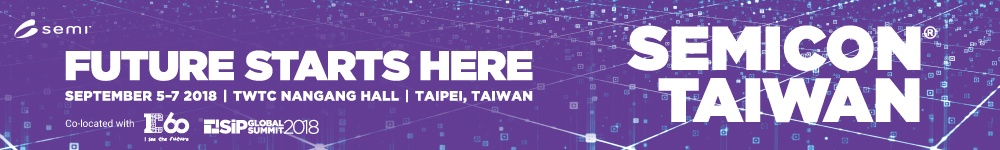
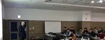
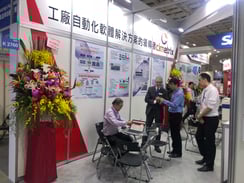
SEMICON Taiwan was held September 5-7, 2018 at the Taipei Nangang Exhibition Center. During that same time (Friday September 7), the e-Manufacturing & Design Collaboration Symposium (eMDC) alsotook place in Hsinchu, Taiwan. Cimetrix exhibited in the Smart Manufacturing Pavilion and had a strong presence at both shows, exhibiting and speaking at SEMICON, and speaking and sponsoring a tea break at eMDC. 

Cimetrix SEMICON attendees included Dave Faulkner (VP Sales and Marketing), Michael Lee (Country Manager Taiwan), Yufeng Huang (Senior Software Engineer), Alan Weber (VP New Product Innovations), Samson Wang (Solutions Engineer) and Kimberly Daich (Marketing Manager); Hwal Song (Country Manager Korea) was also able to attend for one day. We were joined by several partners and distributors as well. The Cimetrix booth was busy throughout the show, and provided a comfortable and convenient setting for the many scheduled and walk-in meetings that took place.

techXspot_taiwan2018_Dave
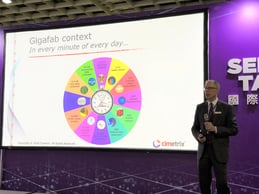
In addition to the exhibitions, SEMICON Taiwan also sponsored many forums for expert speakers throughout the show. Dave Faulkner spoke on Friday morning on the topic of "Making Smart Manufacturing Work with EDA: The Stakeholder-driven requirements Development Process". On that same day, Alan Weber traveled to Hsinchu for eMDC and spoke on a similar topic, "Smart Manufacturing Stakeholders and Their Requirements." Smart Manufacturing is a prevailing topic across the industry and was featured at SEMICON Taiwan, as they continue the Smart Manufacturing Journey that began with SEMICON West. 

Our office in Taiwan has expanded recently with the addition of a new Solutions Engineer, and we are excited as new opportunities open up throughout the region. 

IMG_3881
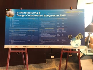
If you would like to learn more about Smart Manufacturing, our work in Taiwan or Cimetrix, please feel free to ask an expert any time. 

Contact Us


Topics: Doing Business with Cimetrix, Events, Global Services, Smart Manufacturing/Industry 4.0

SEMICON Taiwan 2018 is Almost Here!

Posted by Michael Lee; Country Manager Taiwan on Aug 29, 2018 10:48:00 AM

SEMICON Taiwan 2018 is just around the corner. Read the preview now in Chinese or below in English.

semicon taiwan banner

台灣半導體展在台灣微電子生產是一個非常重要的活動。矽美科即將在下週參加此半導體展。展期將由9/5 星期三至9/7星期五,在台北南港展覽館K2760 攤位。台灣半導體提供了一個很好的機會給公司及個人交流的平台,我們非常高興看到我們的客戶及新朋友分享我們的成長。
Cimetrix-Dave-Faulkner-Square

矽美科我們的 銷售和市場部副總裁 Dave Faulkner, 將會在9月7號禮拜五SEMICON TechXPOT演講

若是你有經過我們的攤位K2760, 歡迎你跟我們的專家交流有關連線和相關的需求,我們會在現場做產品演練及介紹和告訴你們我們公司的簡介,你也可以預先來郵件預約,謝謝你。

會議要求


semicon taiwan banner

SEMICON Taiwan is the premier event in Taiwan for microelectronics manufacturing and Cimetrix will be there next week! The show runs from Wednesday, September 5 through Friday, September 7, 2018 at the Taipei Nangang Exhibition Center. SEMICON Taiwan is always a great opportunity to connect with the companies and people in our industry and we are excited to see our clients, meet new people, and share the latest news of Cimetrix products and services with our Taiwan colleagues.

As the semiconductor and microelectronics manufacturing industries grow, SEMICON Taiwan continues to grow as well, both in the number of people who attend and in the number of exhibitors.   This year, Cimetrix will be exhibiting as part of the Smart Manufacturing & Automation Pavilion at Booth K2760. The Smart Manufacturing Pavilion is a great place to start to understand the entire manufacturing process including Front End, Back End and PCB Assembly. Cimetrix-Dave-Faulkner-Square

Cimetrix will also have an expert talk led by Dave Faulkner, Vice President Sales and Marketing, at the SEMICON TechXPOT on Friday, September 7, and we invite you to join us there.

TSIA

On the same day, at the eMDC 2018 event in Hsinchu, our EDA expert, Alan Weber, will deliver a presentation titled Smart Manufacturing Stakeholders and Their Requirements.

Stop by our booth any time to talk to our experts about your specific connectivity and control needs. We will have onsite product demonstrations as well as information about our company available. You can also schedule in advance a time to meet with us at the show by filling out a quick form with your meeting request. 

Meet with Us

Topics: Doing Business with Cimetrix, Events, Smart Manufacturing/Industry 4.0

한국에서의 EDA 연착륙을 위한 3 차 세미나 개최; Hosting the third seminar for soft landing of EDA in Korea

Posted by Hwal Song on Aug 15, 2018 11:04:00 AM

Hwal Song of Cimetrix Korea talks about EDA/Interface A and Korean Equipment Makers. Read now in Korean or below in English.

Koreablog-2

Cimetrix Korea와 국내 파트너사인 링크제니시스는 EDA에 대한 세미나를 7 월 19 일에 개최했습니다. 삼성, SK 하이닉스를 포함한 글로벌 반도체 제조사들이 공정 장비의 추가 통신 프로토콜로 EDA를 채택함에 따라 EDA가 더욱 각광을 받게 되면서 개최한 세번째 세미나였습니다. 지금까지 200 명이 넘는 엔지니어가 이들 세미나에 참석하였으면, 이에 따라 한국에서의 EDA 연착륙이 진행 중입니다. 이들 세미나의 목적은 EDA의 이해부족로 오는 시행착오를 줄이고 첫번째 EDA구현을 가장 빠른 시간에 구현하기 위함입니다.

반도체 제조사의 EDA 채택은 차세대 분석 기능을 구현하고 딥러닝 및 머신 러닝 등과 같은 빅 데이터 및 AI의 새로운 기술을 수용하기 위한 주요 노력의 일환입니다. 대부분의 공정장비들이Freeze II 및 E164가 포함된 EDA 기능의 장착이 요구되거나 요구될 예정이여서,  Cimetrix Korea는EDA의 일반적인 개념뿐만 아니라 심도 있는 구현 방법론에 대한 이해를 위한 도움이 각 장비 제조사의 소프트웨어 엔지니어들에게 필요함을 인지하였습니다. 이러한 요구를 충족시키기 위해 다음과 같이 내용으로 세미나가 준비되었습니다.

Koreablog-1
  • EDA관련 업계 동향 및 채택 현황 -  E164의 중요성 포함
  • 반도체 제조사가 EDA 사양을 어떤 과정을 거쳐 준비하는가?
  • 장비제조사의 소프트웨어팀 관점에서 EDA 구현의 모범 사례와 방법론
  • 여러 장비제조사의 소프트웨어팀을 코칭한 컨설팅 및 지원 팀의 관점에서 EDA 구현 모범 사례와 방법론
  • 구현중이거나 구현된 EDA 적합성 테스트의 모범 사례

활발한 토론과 Q&A를 통해서 한국의 장비 제조사들의 EDA에 대한 높은 관심을 엿볼 수있는 행사였습니다.

궁금한 점이 있으시면 언제든 연락주시기 바랍니다.

Hwal Song


Cimetrix Korea and our local partner, Linkgenesis, held a seminar about SEMI EDA on July 19, the third one since 2016. EDA continues to gain momentum as global chip makers like Samsung and SK hynix have adopted EDA as an additional communication protocol for process tools. So far, over 200 engineers have attended these seminars, promoting the soft landing of EDA in Korea. Their goals include minimizing trial and error due to the lack of understanding on EDA, and speeding up the first deployment of EDA.

Koreablog-2

Adoption of EDA by chip makers is one of the major efforts for factories to implement their next-generation analytic capabilities and also embrace new technologies from big data and AI such as deep learning and machine learning. As most process tools are or will be required to ship with EDA capability, with Freeze II and E164, Cimetrix Korea recognized that Korean software engineers employed at equipment makers were looking for help in understanding in-depth deployment methodologies as well as understanding the general concept of EDA. In order to accommodate these needs, our seminars have been put together with following agenda:

  • General industry trends of EDA and its adoption – the importance of E164
  • Koreablog-1How an EDA specification is put together by a chip maker
  • Best practices & methodologies for implementation of EDA – from the perspective of a software team at a tool maker
  • Best practices & methodologies for implementation of EDA – from the perspective of a consulting and support team who have coached many software teams in tool makers
  • Testing best practices during and after EDA implementation

Active discussions and Q&A showed the high level of interest in EDA among Korean equipment makers. 

Please feel free to contact us whenever you have any questions.

Hwal Song

Topics: EDA/Interface A, Doing Business with Cimetrix, Smart Manufacturing/Industry 4.0

SEMICON West 2018 Pre-Show

Posted by Kimberly Daich; Director of Marketing on Jul 5, 2018 12:29:00 PM

SEMICON West 2018 Beyond SmartSEMICON West 2018 is fast approaching and the Cimetrix team is gearing up for a great show.  The show runs from July 10th – 12th at the Moscone Center in San Francisco and we’re looking forward to meeting with all our present and future clients.

This year SEMICON West is unveiling the new Smart Manufacturing Pavilion to showcase the entire manufacturing process from silicon to systems, including Front End, Back End and PCB Assembly. Cimetrix is excited to announce that we are a sponsor and will be participating in the Smart Manufacturing Pavilion showcase, both as part of the Front End segment as well as in the PCB Assembly area.

The Smart Manufacturing Pavilion includes a “Meet the Experts Theater” featuring presentations from two of our own Cimetrix thought leaders.  Alan Weber will present “Making Smart Manufacturing Work: The Stakeholder-driven Requirements Development Process” on Wednesday, July 11th at 11:00 am. This process has already been used successfully to support the significant growth of SEMI EDA standards usage in Asia, but is equally relevant for a wide range of related Smart Manufacturing technologies.

Later on Wednesday afternoon at 3:00 pm, Ranjan Chatterjee and Dan Gamota of Jabil will present “Convergence of Technologies and Standards Across the Semiconductor, SMT and OSAT Segments.” 

Cimetrix will be exhibiting at booth #1122 in the South Hall, just a short walk from the Smart Manufacturing Pavilion. Stop by our booth or find us at the Pavilion to talk to our experts about your specific needs. We will have onsite product demonstrations as well as information about our company available.  You can also schedule in advance a time to meet with us at the show by filling out a quick form with your meeting request.  

Schedule a Meeting

See you at SEMICON!

Topics: Semiconductor Industry, EDA/Interface A, Events, Smart Manufacturing/Industry 4.0, SMT/PCB/PCBA

That's a wrap - SEMICON China 2018

Posted by Kimberly Daich; Director of Marketing on Mar 22, 2018 10:30:00 AM

semichina1.jpg
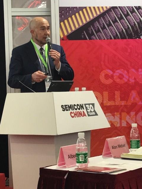
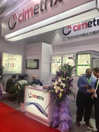
SEMICON China was held from March 14-16, 2018 in Shanghai at the Shanghai New International Expo Centre. Simultaneously co-located at this huge complex were Productronica China and Laser World of Photonics China. All three shows were very busy this year, and it is clear the electronics manufacturing industry in China is booming.

Cimetrix attendees included Dave Faulkner (VP Sales and Marketing), Ranjan Chatterjee (VP Smart Factory Business Unit), Michael Lee (Country Manager Taiwan), Yufeng Huang (Senior Software Engineer), Alan Weber (VP New Product Innovations), and Kimberly Daich (Marketing Manager); Hwal Song (Country Manager Korea) was also able to attend for one day. The Cimetrix booth was busy throughout the show, and provided a comfortable and convenient setting for the many scheduled and walk-in meetings that took place.

Cimetrix partners Facet and Flagship also attended the show, and participated in several customer/prospect discussions. In conjunction with our partner Facet, Cimetrix software products are now used in more than 25 production factories within the China market segment. Moreover, the relationships we have established throughout the semiconductor and electronics markets are strengthening our global presence and enable Cimetrix to provide local support to current and potential clients. The most recent example is our Shanghai office, opened in 2017.

semichina3_alan.jpg

In addition to the exhibitions, SEMICON China sponsored many forums for expert speakers throughout the show. One of these included the New Technology Release Forum where our own Alan Weber was selected as a speaker. His topic “Integrated Equipment Data Collection and Management for Smart Manufacturing” was well received by those in attendance. Smart Manufacturing has been a topic of keen interest at all SEMICONs over the past 18 months, and China was no exception; a separate forum dedicated to Smart Manufacturing drew a standing-room-only crowd to hear a broad range of speakers across the technology spectrum.

We are currently expanding our Shanghai office in response to the exciting growth opportunities we see for our industry in China, and look forward to many years of collaborative work in this region.

Topics: Doing Business with Cimetrix, Events, Global Services, Smart Manufacturing/Industry 4.0

Cimetrix International, Inc., China; 矽美科国际有限公司,中国

Posted by Yufeng Huang; Software Engineer China on Feb 28, 2018 11:40:00 AM

Yufeng Huang of Cimetrix talks about our China Office Opening. Read now in Chinese or English.

美国矽美科股份有限公司上海代表处成立于2017年8月,地址位于称为中国硅谷的上海张江高科技园区。公司总部(矽美科股份有限公司)创建于1987年,地址位于美国犹他州盐湖城。矽美科公司是一家为半导体行业、SMT行业、PCB行业、光伏行业、LED行业及相关行业的设备制造商和生产工厂提供产品和服务的软件公司。

China_office_1.pngChina_office_2.jpg

矽美科公司有着非常良好的客户评价,公司不仅将自己视为客户的重要供应商,更加将自己视为客户值得信赖的合作伙伴。我们坚信有能力为客户提供全球最先进的基于SEMI标准的软件解决方案。

矽美科上海代表处为中国、台湾等亚太地区客户提供售前产品咨询,客户培训,售后技术支持服务。我很荣幸在今年8月份加入到矽美科上海代表处,在过去的几个月内我们不断收到老客户给予的好评和新客户的合作意向。感谢新老客户对公司的支持,我们将一如既往的为客户提供最优质的、高效的服务,希望我们的产品和服务能让您满足,并为您带来巨大的帮助。

美国矽美科股份有限公司上海代表处
地址:上海市浦东新区盛夏路399弄1号(A座)3楼328室3069单元 (邮政编码201210)
技术联系:黄玉峰
电话:+86-21-8022-0935

销售联系:Michael Lee
电话:+886-926395649


American Cimetrix Incorporated Shanghai Representative Office was established in August 2017. It is located in ZhangJiang High-Tech Park, which is also known as China’s Silicon Valley. The headquarters of Cimetrix, Inc, founded in 1987, is located in Salt Lake City, Utah, USA. Cimetrix is a software company that provides software products and services to OEMs and Fabs in the semiconductor, SMT, PCB, photovoltaic, LED and related industries.

Enjoying excellent customer reputation, Cimetrix considers itself more as customer’s trusted partner than customer’s supplier. We firmly believe that we have the ability to provide customers with the world's most advanced SEMI-based software solutions.

Cimetrix Shanghai Representative Office provides pre-sales consulting, customer training, after-sales technical support services to mainland China, Taiwan and other Asia areas. I am greatly honored to join Cimetrix Shanghai Representative Office in August 2017. In the past few months, we have continuously received favorable comments from existing customers and cooperation intentions from potential customers. Thanks for their trust and support of the company, we will, as always, provide our clients with the best and most efficient services. We believe that our products and services will meet customer satisfaction and greatly enhance your product quality.

American Cimetrix Incorporated Shanghai Representative Office
Address: Unit 3069, Room 328, Floor 3, No. 1 (Block A), Lane 399, Shengxia Road, Pudong New Area, Shanghai (Post Code: 201210)

Technical Contact: Yufeng Huang
Telephone: +86-21-8022-0935

Sales Contact: Michael Lee
Telephone: +886-926395649


Topics: Doing Business with Cimetrix, Global Services, Smart Manufacturing/Industry 4.0