When I posted a blog back in April, I wrote about the change in the industry outlook over the previous six months. In October 2012, the semiconductor equipment industry looked as if it was going to go into a decline, perhaps a steep decline, but by January 2013, the outlook looked brighter. By March 2013, industry analysts were predicting 2013 would be down, but not as badly as analysts originally thought. Still, TSMC was reporting they are adding capacity and Applied Materials announced they were on an up cycle. In addition, the forecast for 2014 was looking bright, with predictions of healthy growth.
As we move into the third quarter of 2013, the expectation is that semiconductor equipment total year revenues will decline somewhere between 1.5% and 7.5% from the $36.9 million in 2012. We are seeing equipment suppliers being a bit cautious about Q3 of this year. Several companies are offering guidance of no growth this quarter.
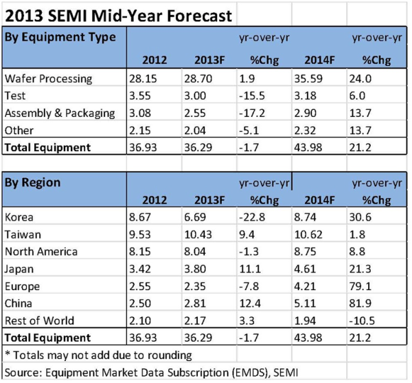
The forecast for 2014 continues to be upbeat, with SEMI expecting equipment revenue up by 21% and VLSI Research calling for a 27% increase. The majority of that growth will be in wafer processing equipment, which is expected to increase by 24% from 2013 levels.
Here is the chart provided by SEMI in July (see SEMI Sees 21% Increase in Chip Equipment Spending for 2014):
Another encouraging sign is the SEMI North American book-to-bill ratio has remained above 1 for the past six months (see North American Semiconductor Equipment Industry Posts June 2013 Book-to-Bill Ratio of 1.10).
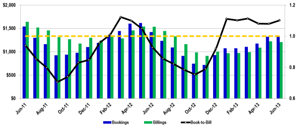
North American Semiconductor Industry Bookings and Billings ($M)
The above chart shows that bookings have been going up since November 2012, and, since January 2013, more orders were received compared to products that were shipped, meaning that the industry is growing.
The question is “What is fueling this drive to build more capacity?” The answer is demand for mobile computing and communication. SIA (the Semiconductor Industry Association) announced worldwide sales of semiconductors in May 2013 of $24.70 billion, an increase of 4.6%. That is the largest sequential monthly increase in sales for the industry since March 2010.
IDC forecasts the mobile wireless communication segment will grow over 10% in 2013, and the consumer segment, including tablet computers, e-readers, set top boxes, and DVD recorders, will grow over 15% this year. Even automobiles are getting smarter, and semiconductor content will grow over 5% in vehicles this year (see IDC Forecasts Worldwide Semiconductor Revenue Will Grow 6.9% and Reach $320 Billion in 2013).
We are in a cyclical industry, and we know that what goes up must come down. If the analysts are correct, next year should be a robust year for semiconductor equipment makers. We will keep you posted on what we are seeing in the semiconductor equipment industry.