SEMICON Taiwan 2018 is just around the corner. Read the preview now in Chinese or below in English.
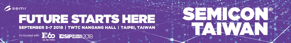
台灣半導體展在台灣微電子生產是一個非常重要的活動。矽美科即將在下週參加此半導體展。展期將由9/5 星期三至9/7星期五,在台北南港展覽館K2760 攤位。台灣半導體提供了一個很好的機會給公司及個人交流的平台,我們非常高興看到我們的客戶及新朋友分享我們的成長。
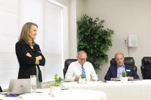
矽美科我們的 銷售和市場部副總裁 Dave Faulkner, 將會在9月7號禮拜五SEMICON TechXPOT演講。
若是你有經過我們的攤位K2760, 歡迎你跟我們的專家交流有關連線和相關的需求,我們會在現場做產品演練及介紹和告訴你們我們公司的簡介,你也可以預先來郵件預約,謝謝你。

SEMICON Taiwan is the premier event in Taiwan for microelectronics manufacturing and Cimetrix will be there next week! The show runs from Wednesday, September 5 through Friday, September 7, 2018 at the Taipei Nangang Exhibition Center. SEMICON Taiwan is always a great opportunity to connect with the companies and people in our industry and we are excited to see our clients, meet new people, and share the latest news of Cimetrix products and services with our Taiwan colleagues.
As the semiconductor and microelectronics manufacturing industries grow, SEMICON Taiwan continues to grow as well, both in the number of people who attend and in the number of exhibitors. This year, Cimetrix will be exhibiting as part of the Smart Manufacturing & Automation Pavilion at Booth K2760. The Smart Manufacturing Pavilion is a great place to start to understand the entire manufacturing process including Front End, Back End and PCB Assembly.
Cimetrix will also have an expert talk led by Dave Faulkner, Vice President Sales and Marketing, at the SEMICON TechXPOT on Friday, September 7, and we invite you to join us there.

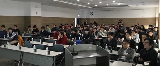
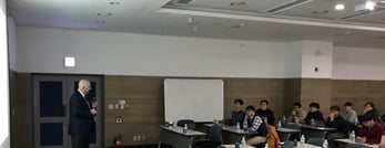
On the same day, at the eMDC 2018 event in Hsinchu, our EDA expert, Alan Weber, will deliver a presentation titled Smart Manufacturing Stakeholders and Their Requirements.
Stop by our booth any time to talk to our experts about your specific connectivity and control needs. We will have onsite product demonstrations as well as information about our company available. You can also schedule in advance a time to meet with us at the show by filling out a quick form with your meeting request.


 How an EDA specification is put together by a chip maker
 Meet David Harrison, Quality Engineering Team Lead. Read on to learn a little bit more about David.
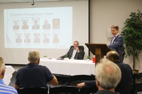
 Cimetrix is here at SEMICON West 2018 and we're excited to be a part of the first Smart Manufacturing Pavilion in the South Hall. We hope you've been able to drop by and hear some of the great speeches including our own experts Alan Weber, VP New Product Innovations and our VP & GM Smart Factory Business Ranjan Chatterjee with Dan Gamota (VP Digital Engineering Services) at Jabil.
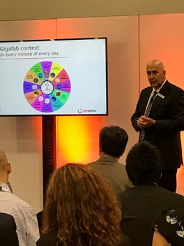 The question now becomes “How DO the industry’s leading manufacturers ensure the equipment they buy will support their Smart Manufacturing objectives?” This presentation explains how the careabouts of key stakeholder groups are “translated” into specific equipment automation and communications interface requirements which can then be directly included in the equipment purchasing specifications. As more semiconductor manufacturing companies take this approach, effectively “raising the bar” for the entire industry, the collective capability of the equipment suppliers will increase in response, to everyone’s benefit.
 SEMICON West 2018 is fast approaching and the Cimetrix team is gearing up for a great show. The show runs from July 10th – 12th at the Moscone Center in San Francisco and we’re looking forward to meeting with all our present and future clients.

 The Quality Software Engineering team at Cimetrix is dedicated to delivering the highest quality software products to all Cimetrix customers. The QE team works closely with the development engineers to plan and build sound, testable solutions in an agile working environment. Through rigorous testing and creative problem solving, we advocate for and build quality into our products. We accomplish this with a determined team that works hard to uphold high standards of both software functionality, and software structure.
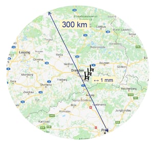
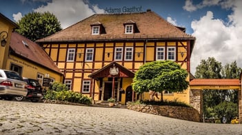
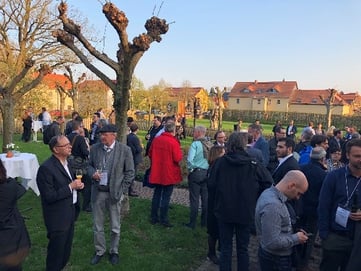
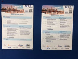
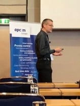
 Cimetrix participated in the recent European Advanced Process Control and Manufacturing (apc|m) Conference, along with over 160 control systems professionals across the European and global semiconductor manufacturing industry. The conference was held in Dresden, a beautiful city in the Saxony state of Germany which was the site of the original European conference in 2000 and host to this annual event many times since.
 “FDC to the power of 2 – how it got us to the next level of manufacturing excellence“ by Jan Räbiger of GLOBALFOUNDRIES – one of a number of long-time thought leaders in the development and application of APC technology, Jan described the latest phase of FDC system evolution, which includes broad use of the EDA/Interface A standards to zero in on recipe step-specific anomalies that had previously escaped detection.