The focus of the most recent SYSTEMA Expert Day, held during a snowy week in Dresden in late January 2016 in conjunction with the 13th annual innovationsforum, was “200mm Fab Enhancement” and featured a number of presentations from Systema GmbH customers and partner companies.
By way of background, there are a number of reasons for the emphasis on 200mm fab enhancement, most notably that many of these factories are enjoying a renaissance of business to meet the growing demands for IoT (Internet of Things) devices. Moreover, since the drivers for this market segment include cost, variety, and volume, the automation and operations people in these factories are faced with a new combination of challenges not seen in earlier markets.
Cimetrix’ contribution to the event was a presentation titled “Equipment Data-Driven Continuous Improvement for 200mm Fabs,” which outlined a model-based, ROI-driven approach for adding equipment data collection capabilities to existing factories. Our basic premise is that such an approach helps meet some of the automation challenges in an incremental, cost-effective way without requiring major redesign of the factory or equipment control systems.

Since the term “model” is used in many different contexts, we first clarified what this term means in the context of SEMI equipment communications standards, and how this evolved over the past three decades. This was accomplished using a natural language analogy, which is shown in the figure below. Note that the culmination of this process to date is the EDA (Equipment Data Acquisition) metadata model called for in the latest generation of standards, which is very prescriptive in terms of structure, content, and naming conventions for the elements of a semiconductor manufacturing equipment. And even thought the specifics of this model were designed with 300mm wafer fab equipment in mind, the principles well apply to all substrate sizes, and even to the types of material, processes, and equipment found in back end assembly and test factories.
After establishing the value of explicit models for representing equipment, sensors, and other key items in a manufacturing environment, we next introduced concept of an ROI-driven strategy for evaluating the relative benefit of various data collection projects. This strategy first identifies and ranks the key manufacturing objectives that must be addressed, then poses the questions that must be answered to meet those objectives. It then identifies the data sources for the information required to answer those questions, and the data collection techniques (including software) applicable to those sources. Finally, since the original objectives can change with time and additional knowledge, they should be re-examined periodically, giving the strategy an iterative aspect as well.
In order provide specific examples for the uses of equipment data in a continuous improvement program, the presentation listed a number of application use cases that have been successfully deployed in 200mm facilities. These included (in general increasing order of complexity) substrate tracking, process execution tracking, product time measurement (aka wait time waste analysis), external sensor integration, component fingerprinting, and product traceability.

A couple of these were then explained in more detail, showing how a basic tracking application could start by using a small subset of the equipment data, and then evolve over time to provide more advanced functions (and benefit!) as more detailed information was made available.
For those who want to understand this process in more depth, you are welcome to download the entire presentation using the link below, or call us to discuss how we can apply these ideas to your company!♦
“Equipment Data-Driven Continuous Improvement for 200mm Fabs"


 Linkgenesis will be exhibiting at SEMICON Korea 2016, which will be held in Seoul on January 27-29. Please stop by our booth in Hall C #1739 to see our product line as well as Cimetrix’ CIMPortal Plus, and discover how our software brings the latest innovations to the semiconductor manufacturing industry.
 Many software companies can do this is through the way they use software versioning. It is common for software companies to use a major.minor.patch.build software versioning scheme, for example iTunes 12.3.1. This type of software versioning allows the software company to communicate the scale and impact of the changes in the release to their customers. A change in the “major” release number indicates to customers that there are some significant changes in this release that may impact the way it interacts with the product. The customer will likely need to make code changes or procedural changes when upgrading to such a release. A change to the “minor” release number denotes that there are multiple changes in the release, but customers should see only minor, or possibly no changes, in the way they use the product. A minor release may include some small new features that could potentially require code changes if the customers wants/needs those new features. A “patch” release is generally used to address a specific issue and should not change the customer experience with the software. The build number is most often provided to help the software company when researching a question or customer reported defect.
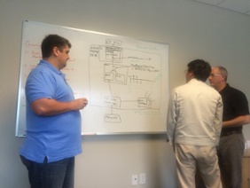 For a small company like Cimetrix, we can be proud of these accomplishments. We are very thankful to have had


 However, before diving into a detailed design process for an EDA factory system, you must decide what overall system architecture will govern that design. A number of factors go into this decision, including 1) the functional requirements that distinguish EDA-based data collection from other more traditional approaches, 2) technology constraints of the existing factory systems, 3) budget limitations, 4) schedule requirements, and especially 5) the non-functional requirements (scalability, performance, reliability, ease-of-use, etc.) that often make the difference between success and failure of a given system.
 Moreover, when communicating these requirements to the OEM community, it is useful to explain what strategic manufacturing objectives are being addressed and what the information will be used for; this context helps the suppliers understand why the specs may include a high level of detailed information, and can shift a potentially adversarial negotiation process more towards a teaming relationship based on shared objectives.