Industry News, Trends and Technology, and Standards Updates

29th Advanced Process Control Conference Retrospective: Still serving the industry’s APC community after 25+ years

Posted by Alan Weber: Vice President, New Product Innovations on Nov 8, 2017 10:43:00 AM

APC 2017 Conference Austin TXAustin, Texas was the site of this year’s conference, going back to its roots after almost 30 years. Because of its unique focus on equipment and process control technology for the semiconductor industry, and the consistently high quality of its technical content, this conference continues to attract both industry veterans and newcomers to this domain, with this year’s attendance over 160.

APC2017_2-557375-edited.jpgAPC2017_3.jpg

Cimetrix has been a regular participant and presenter at this event, and this year was no exception. Alan Weber made a presentation entitled “ROI-based Approach for Evaluating Application Data Collection Use Case Alternatives” that was jointly developed with Mark Reath of GLOBALFOUNDRIES. The key message of this talk was that data collection should not be viewed as an all-or-nothing proposition but rather a spectrum of alternatives within which an approach can be chosen that best fits the problem to be addressed. As examples, the presentation described specific FDC use cases that resulted in significant savings through reduced false alarm rate and fewer/less severe process excursions. For a copy of this presentation, follow the link at the bottom of this posting.

apc2017_5.pngBoyd Finlay’s (GLOBALFOUNDRIES) keynote presentation was undoubtedly one of the highlights of the conference. His presentation, “Raising the Bar: Foundry Expectations for Equipment Capability and Control,” painted a compelling picture of how future semiconductor manufacturing equipment must be able to support the growing demand for semiconductors in almost all aspects of modern life, especially in self-driving cars and their supporting infrastructure. For example, one of the specific expectations is that “Fab engineers expect fully integrated instrumentation on and around equipment to provide well established unambiguous high-volume manufacturing sensor supporting BKMs (best-known methods).” This presentation is well worth your time to review regardless of your job function in the industry, so follow the link below for a copy.

Samsung also offered some very interesting insights in a presentation titled “Wafer Level Time Control for Defect Reduction in Semiconductor Manufacture FABs.” It correlated defect densities to position in the FOUP and explained 2 sources for these: 1) outgassing of wafers after certain kinds of processes (which can be addressed with N2 purging), and 2) the difference in post-process waiting time, which must now be considered at the individual wafer level rather than the lot as a whole.

This conference and its sister conference in Europe are excellent venues to understand what manufacturers do with all the data they collect, so if this topic piques your interest, be sure to put these events on your calendar in the future. In the meantime, if you have questions about any of the above, or want to know how equipment connectivity and control fit into the overall Smart Manufacturing landscape, please contact us!

Boyd Finlay's presentation

Alan Weber's presentation


Topics: EDA/Interface A, Doing Business with Cimetrix

Sending data in chunks to optimize network performance

Posted by Derek Lindsey: Product Manager on Oct 19, 2017 10:11:00 AM

The Interface A / EDA standards define powerful methods for collecting data from an equipment control application. The data collection can be as simple as querying values of a parameter or two, or as complex as gathering thousands of parameter values across multiple reports. EDA specifies the use of internet standard messaging protocols like HTTP, XML and SOAP messages for collecting this data.

It is possible to define so many data collection plans gathering so much data that the sheer amount of data causes network performance to degrade. To remedy this situation, the EDA standards provide ways of sending the data in “chunks,” which dramatically improves the performance of XML over HTTP.

Two methods for sending data in chunks are grouping and buffering.

Grouping

Grouping only applies to individual Trace Requests within a Data Collection Plan (DCP).  If I have a trace request with an interval of one second, a group size of 1 would generate a report every second and send it across the wire. If I change my group size to 10, a report would still be generated every second, but the report would not be sent across the wire until 10 reports have accumulated. Each report has its own timestamp and they are arranged in the order they occur. The following diagram shows a trace data collection report with a group size of 3.

EDAdatachungs-1.pngBuffering

Buffering is different from grouping in that the buffer interval (in minutes) applies to an entire DCP rather than individual trace requests within that plan. For example, if I have a DCP with three trace requests and two event requests defined with a buffer interval of 1 (meaning one minute), the trace reports would still be generated at the specified trace interval. Event reports would be generated as the events are triggered. The reports are not sent to the EDA client until the buffer interval expires. At that point, all the data reports that were generated within that buffer interval time are packaged and sent to the EDA client.EDADatachunks-2.png

Combining Grouping and Buffering

Grouping and buffering can be combined as well. Groups are still defined on a per trace basis. If a group size has not been met when the buffer interval expires, the group report will be in the next buffer report that is sent.

Summary

With the provision for transmitting data in blocks, using grouping for trace data reports and/or buffering for all data reports, EDA is well suited for collecting large amounts of data without having a negative effect on network performance.  

Topics: EDA/Interface A, Data Collection/Management

Traceability Application Support: Episode 4 in the “Models in Smart Manufacturing” Series

Posted by Alan Weber: Vice President, New Product Innovations on Aug 1, 2017 11:15:00 AM

chicken_or_egg.jpg…never mind which came first… do you know where the chicken and the egg came from?

As integrated circuits increasingly find their way into applications for which human and environmental safety are paramount, the regulatory requirements related to product traceability become ever more stringent. For example, the automotive industry already requires that a device maker be able to provide a full manufacturing process history within 48 hours of a request for certain kinds of products, but this only scratches the surface of what’s to come in the growing markets for autonomous vehicles and their supporting public infrastructure, aircraft components, medical implants and diagnostic systems, and the like.

semiconductor_manufacturingThe good news in all this is that the latest semiconductor manufacturing equipment interface standards include enough information about the product being built and the processes used at each step along the way to directly support these traceability requirements with little or no custom software. Specifically, the SEMI Equipment Data Acquisition (EDA) suite of standards (also known as “Interface A”) defines the components of an explicit equipment model that can represent this information, and the SEMI E164 (EDA Common Metadata) standard goes so far as to specify the actual structure and naming conventions for the required components.

Before getting deeper into the specifics, let’s step back and define “traceability” in this context. According to ISO 9000 (Quality management systems – Fundamentals and vocabulary), the term means “the ability to trace the history, application or location of an entity by means of recorded identifications.” 

In a wafer fabrication facility, this definition covers a broad range of capabilities. The most basic interpretation could be satisfied by simply having an ordered list of the manufacturing equipment visited by each wafer (substrate) during its 3-month journey through the fab. As long as the manufacturer keeps a record of which substrate each assembled die came from (which most do), the required documentation could be generated from information contained in the MES (Manufacturing Execution System) and its associated scheduling/dispatching system. 

Symptoms_Problems_Cause_tree

However, at the other end of the spectrum, the traceability requirement may include not only the list of equipment visited, but also the recipe used at each equipment, the precise timing of wafer movement and process modules visited within the equipment, values of any adjustable recipe parameters and/or equipment constants that affect process behavior, batch identification and status information for any consumables used during the process, usage counts for any fixtures involved, operator interactions (if any), and so on. The reason for this level of detail is to enable the failure analysis engineers to identify the potential root causes for any field failures, and then determine what other devices in the field may be susceptible to similar failure conditions for product recall purposes.

To be sure, much of this information could be assembled after-the-fact from the various data bases maintained by the equipment and process engineering and yield management systems present in most modern wafer fabs, but this process can be complex, time-consuming, and error-prone. A better approach would be to generate the most commonly needed traceability records on-the-fly directly from information available in the equipment... and this is where the newest EDA standards enter the picture. 

By analogy, let’s look at an intuitive example: a commercial cake baking enterprise. Even for a relatively simple (compared to semiconductor manufacturing) production process, full traceability requires information from the raw materials suppliers through the manufacturing process to packaging and finished goods warehousing. You can see in the picture below that material, recipe, and equipment setup information is included in the records produced.

Complete Production Traceability

In a unit of semiconductor manufacturing equipment with an E164-compliant interface, these types of information appear in various sections of the equipment metadata model. Specifically, material-related information is captured in the “Material Manager” logical component, shown in expanded view below* to highlight the state transition events and parameter data available for each substrate during its transportation and processing in the equipment.

Material_Manager_component

Recipe-related information is found in the physical modules responsible for substrate processing (“ProcessingChamber1” and “ProcessingChamber2” in the example below), within the “E157-0710:ModuleProcess” state machine, dictated by the SEMI E157 (Module Process Tracking) standard and required by E164. Note the rich list of context information available at every recipe step, including the RecipeParameters array, in the expanded model excerpt below. RecipeParameters_arrayTaken together, the timing and parameter data from these two sections of the equipment model supply most of the information required for full wafer fab traceability. Moreover, since SEMI E164 actually standardizes the event and parameter names in the model, the DCPs (data collection plans) that collect this information can be programmatically generated and activated for all the equipment that is E164-compliant. This represents a significant engineering cost reduction over the conventional methods used to identify, collect, and manage this information. The figure below is one visualization of such a DCP.DCP_Visualization

When extended beyond individual devices to circuit boards, modules, and completed parts (see the example below for an automobile speedometer), these requirements require even more bookkeeping… but that’s a topic for another day!automobile_speedometer

This article is the fourth in the series recently announced in the Models in Smart Manufacturing Series - Introduction, be sure to watch for subsequent postings that will expand on this theme. 

We look forward to your feedback and to sharing the Smart Manufacturing journey with you.


*The visualizations of equipment metadata model fragments and DCP contents are those produced by the Cimetrix ECCE Plus product (EDA Client Connection Emulator).

Topics: EDA/Interface A, Models in Smart Manufacturing series, Smart Manufacturing/Industry 4.0

EDATester Product Launch: EDA/Interface A Freeze II Testing

Posted by Jesse Wright; Software Engineer on Jul 25, 2017 11:30:00 AM

In a world of automated equipment, having tools to automate the testing of an equipment’s implementation of the SEMI EDA (Equipment Data Acquisition) standards (also known as Interface A) is invaluable. Cimetrix is proud to announce an integrated solution that supports the broadest range of use cases in EDA/Interface A testing - the Cimetrix EDATester™. EDATester is a tool that will help organize, streamline, and automate the testing process while also providing other analytical capabilities. 

Cimetrix knows that testing an equipment interface is not simply a one-time event; rather, tests should be performed in the OEM’s facilities throughout the development process and before final shipment, upon delivery to the customer’s factory, and even after the equipment has been placed into full production. Cimetrix EDATester is designed to do exactly that.

EDATester4.png

What do we really mean by “testing?” What are we testing? Since the scope is very broad, let's frame the answer in a few distinct categories.

Compliance Testing

Does the equipment’s EDA interface behave correctly based on the SEMI E120, E125, E132, and E134 standards and all the services defined therein? To answer this question, we make use of the ISMI EDA Evaluation Method. This document contains a set of functional evaluation procedures that “tests” the equipment’s implementation of the standards. These procedures check for things like ACL privileges and roles, establishing and terminating communications sessions, managing (or preventing the management of) Data Collection Plans (DCPs), and even looking for the proper notification of metadata revisions. If everything works as expected in these procedures, that equipment would be deemed “compliant.”

EDATester uses ISMI’s functional evaluation procedures as guidelines, and implements tests that are automated for all client-side actions. A process that might have taken multiple days to execute manually can be done in minutes, even when some interaction with the equipment itself is required; the fully automated tests that require no user interaction with the equipment can be run in seconds.

Performance Testing

Everything might look great on the client side with the ability to define a DCP, activate it, and start receiving data; but how many DCPs will the equipment actually support? How fast can I sample the parameters I want to collect in my Trace Requests without overloading the equipment’s EDA interface? Even if I could do this manually, how would I begin to answer this question?

EDATester automates multiple iterations of performance testing using different variations of DCPs while analyzing the timestamps of the E134NewData messages to determine the integrity of the actual sampling rate. Having such tests helps you determine whether the equipment can handle a new DCP in response to a process engineering request, or if the equipment supports the full range of performance requirements agreed to in the purchasing specifications. To this end, you can specify testing configurations for things such as:

  • Number of simultaneously active DCPs 
  • Trace Request Sampling Interval
  • Number of parameters per Trace Request
  • Group Size for message buffering
  • Timing tolerance for expected vs. reported Data Collection Report (DCR) timestamps

Conformance Testing

The testing tool in practical use across the industry for measuring an equipment’s conformance to the SEMI E164 EDA Common Metadata standards is called the Metadata Conformance Analyzer (MCA). It uses a set of .xml files describing the metadata model as input, analyzes the model according to the requirements of E164, and provides feedback.

EDATester currently generates the .xml input model files required by the MCA, and may eventually incorporate the model conformance testing functions as well.

Summary

Having the correctly sized wrench when you need to apply the proper torque to a bolt is helpful and sometimes necessary—at least you can get the job done. But when you have hundreds of bolts to insert and tighten precisely, wouldn’t you rather have an adjustable ratchet? Or an air ratchet?

Whether it’s to test and characterize the EDA interface on a new equipment type,  verify that a software update to a production piece of equipment has been installed correctly, or debug an interface performance issue that has somehow arisen in production, the Cimetrix EDATester is the right tool to have in your arsenal to quickly, effectively, and thoroughly “test” an equipment’s EDA interface capabilities. Don’t waste another day with manual processes that leave you guessing. Get in touch with us today to find out more about the EDATester product. 

Topics: EDA/Interface A, Cimetrix Products

Implementing CIMPortal Plus

Posted by Derek Lindsey: Product Manager on Jul 7, 2017 12:07:00 PM

Toolkit.jpg

Generally, when I do a DIY (do-it-yourself) project around the house, I spend the majority of the time searching for my tools. The other day I was helping a friend with a project. He had a well-organized tool box and it seemed that the perfect tool was always at his fingertips. I was amazed at how fast the project went and how easy it was when the right tools were handy.

In April of 2016, we published a blog called OEM EDA Implementation Best Practices that outlined ten things to consider when designing an equipment-side EDA / Interface A solution to fit your needs. This blog post analyzes a few of those recommendations and looks at how using the Cimetrix EDA products CIMPortal Plus, ECCE Plus and EDATester (a well-stocked and organized tool box) makes it very easy to follow those recommendations.

The basic steps in creating a useful EDA implementation are:

  1. Determine which data will be published
  2. Build an equipment model
  3. Deploy the model
  4. Publish the data from the equipment control application
  5. Set up a data collection application
  6. Test the interface

The blog post mentioned above states, “Since the content of the equipment metadata model is effectively the data collection contract between the equipment supplier and the factory users, your customer’s ultimate satisfaction with the EDA interface depends on the content and structure of this model.” Before building your model, you need to determine what data the equipment will make available for collection. CIMPortal Plus has the concept of a Data Collection Interface Module (DCIM) that publishes this data to the EDA server. The engineer building the model will map the data from the DCIM into the equipment model.

Once the mapping of the data is complete, the engineer will need to put this data in a format understood by the server. CIMPortal Plus provides a utility called Equipment Model Developer (EMDeveloper – pictured below) that makes it easy to create the hierarchy of your equipment (SEMI E120) and embed the data from the DCIM into that model (SEMI E125). If you use the tools and best practices provided in EMDeveloper, your equipment model will conform to the SEMI E164 (EDA Common Metadata) standard as well. This can be very useful when writing data collection applications so conformance to E164 is being required by more and more fabs. The E164 standard was developed to encourage companies using Interface A connections to provide a more common representation of equipment metadata based upon the SEMI E125 Specification for Equipment Self-Description. This makes data collection more uniform across these pieces of equipment.

CIMPortalPlus_Blogimage1.png

Once the model is created and validated, it is deployed to the CIMPortal Plus server. The server is the component that manages and tracks all data collection plans, reports, tasks, access control and timing. 

With the DCIM information embedded in the model (described above), it is easy for the equipment control application to push the data to be published to the EDA server for collection. This is done by using a simple API available on the DCIM interface.

In addition to CIMPortal Plus server capabilities, Cimetrix has other products available to help with client-side data collection. ECCE Plus is an industry approved method for manually testing EDA implementations. For users who need to create client-side data collection applications, Cimetrix also provides EDAConnect - a powerful library that handles all the connection details and allows developers to concentrate on the specific data collection and analysis tasks.

Fabs receive a wide variety of equipment with EDA implementations from numerous vendors. They want to use a single verification application to make sure that all EDA implementations are compliant to the EDA standards. That’s where EDATester comes in. EDATester is a new product that allows users to quickly and accurately verify EDA standards compliance by automating the test procedures ISMI EDA Evaluation Method that were defined specifically for this purpose. If you use Cimetrix products to implement your EDA interface, you are guaranteed to be compliant with the SEMI EDA standards. But whether you use Cimetrix products to implement your EDA interface or not, you (and your fab customer) want to rest assured that your implementation is fully compliant. Moreover, you’ll want to know that you’ve met the fab’s performance criteria for your equipment interface. To support this use case, the EDATester also allows users to quickly profile the performance of EDA data collection on a piece of equipment so that fabs and those using the data will know the boundaries within which they can successfully collect equipment data.

With the well-stocked EDA tool box provided by Cimetrix, following the EDA best practices in creating an efficient, standards-compliant EDA interface becomes a snap.

Topics: EDA/Interface A, Cimetrix Products

Precision Data Framing during Process Execution – Tricks of the Trade: Episode 3 in the “Models in Smart Manufacturing” Series

Posted by Alan Weber: Vice President, New Product Innovations on Jun 27, 2017 11:30:00 AM

…or how to move away from “just in case” data collection...

It’s a common process engineering request of the manufacturing IT folks: “Please collect as much data as you can during this process, and we’ll figure out what’s important later.” And this approach has worked fairly well up to this point. However, with 10nm (and below) production on the horizon, coupled with the desire to sample key parameters at ever-increasing rates, the amount of on-line data storage required to support this approach could skyrocket… to say nothing of the difficulty in sifting through all that data to extract the real information you wanted in the first place.

Models3.1.jpgModels3.2.jpg

Fortunately, you don’t have to look very far into the SEMI EDA (Equipment Data Acquisition) standards (also known as “Interface A”) to find an excellent solution alternative. The portion of the standard equipment metadata model (specified by SEMI E164 – EDA Common Metadata) that deals with process execution (SEMI E157 – Process Execution Tracking) combined with the conditional triggering features of Trace Requests (SEMI E134 – Data Collection Management) enables a process engineer to precisely collect the right data at the right time at the right frequency without over-burdening the equipment or factory systems by collecting and storing less important data at the highest rates. 

Let’s look at an example. The key state machine called for in the E157 standard (see figure below*) has 2 major states (NOT EXECUTING and EXECUTING) with intuitive transition events defined between them (Execution Started, Execution Completed, and Execution Failed). If you only care about tracking the overall execution time of the process recipes on a given tool, then a single DCP (Data Collection Plan) with a pair of Event Requests on the Started and Completed events is all you need. The difference in the timestamps of the corresponding Event Reports provides the necessary information. 

Models3.3.png

However, if you want to monitor a baseline set of equipment performance parameters at a low frequency (say, 1 Hz) throughout the recipe, and collect the key parameters for analyzing process behavior at a higher frequency (50 Hz) during the most critical process steps (5 through 8), you would use a DCP with multiple Trace Requests triggered by the Step Started and Step Completed transition events between the two sub-states (GENERAL EXECUTION and STEP ACTIVE) of the EXECUTING state. Furthermore, you would use the conditional triggering feature of the Freeze II version of the EDA standards (SEMI E134-0710 or later) to produce Trace Reports only during the critical process steps. The figure below is one visualization* of such a DCP.

Models3.4.png

You may have noticed from this example that multiple triggering conditions are ANDed together to determine whether or not to collect the data and generate a Trace Report. But how do you handle the situation in which OR functionality is needed to produce the desired result, for example, in the case that multiple sets of recipe steps are considered critical (say, steps 5-8 and steps 11-13)?

This is where you can use one of the “tricks of the trade.” Simply define multiple Trace Requests with different sets of ANDed conditions to cover the range of ORed situations. For the case above, you would need two Trace Requests: one for each critical set of contiguous recipe steps (see visualization below).

Models3.5.png

Note finally that you can also apply comparison operators to analog values to trigger Trace Requests, which may be especially useful to sample specific parameters when some value crosses an important threshold. 

Models3.6.png

Taken together, these techniques are sometimes called “data framing,” which is an important tool in the controlling the scope of factory data explosion that will soon be upon us. 

This article is the third in our Models in Smart Manufacturing series – be sure to watch for subsequent postings that will expand on this theme.

We look forward to your feedback and to sharing the Smart Manufacturing journey with you.

*The visualizations of equipment metadata model fragments and DCP contents are those produced by the Cimetrix ECCE Plus product (EDA Client Connection Emulator).


Topics: EDA/Interface A, Models in Smart Manufacturing series, Smart Manufacturing/Industry 4.0

European Advanced Process Control and Manufacturing Conference XVII: Retrospective and Invitation

Posted by Alan Weber: Vice President, New Product Innovations on May 17, 2017 11:30:00 AM

APC.jpgCimetrix participated in the recent European Advanced Process Control and Manufacturing (apc|m) Conference, along with over 150 control professionals across the European and global semiconductor manufacturing industry. The conference was held in Dublin, a lively city on the east coast of Ireland which features a charming juxtaposition of old and new and is home to 1.2 million of the friendliest and most talkative people on the planet! 

APC_2017_1.jpg

Of course, one of Ireland’s greatest “natural resources” may also contribute to their fine spirits…

APC_2017_2.jpg

This conference, now in its 17th year and organized by Silicon Saxony, is one of only a few global events dedicated to the domain of semiconductor process control and directly supporting technologies. This year’s attendance was up from that of the three previous years, a clear indication that this area continues to hold keen interest for the European high-tech manufacturing community. Moreover, the participants represented all links in the semiconductor manufacturing value chain, from universities and research institutes to component, subsystem, and equipment suppliers to software product and services providers to semiconductor IDMs and foundries across a wide spectrum of device types to industry trade organizations – something for everyone.

APC_2017_3-1.jpg

The local sponsor for the conference was Intel, which is the largest private-sector investor in the Irish economy and one of its biggest employers. In addition to excellent logistics support, Intel hosted a lovely evening of fine food and local entertainment at the world-renowned Trinity College.

APC_2017_4.1.pngAPC_2017_5.png

As in many prior years, Cimetrix was privileged to present at this conference. Alan Weber delivered a talk entitled “Smarter Manufacturing with SEMI Standards: Practical Approaches for Plug-and-Play Application Integration.” This topic was well aligned with one of the key themes of this year’s event, but stressed the point that our industry already has at its disposal many of the tools, techniques, and enabling standards required for Smart Manufacturing. Specifically, the presentation illustrated how the new SEMI E172 SECS Equipment Data Dictionary (SEDD) standard could be used to document an equipment’s GEM interface in way that provided much of the same hierarchical structure and context information inherent in the latest generation of EDA metadata models (SEMI E120, E125, and E164). If you want to know more, feel free to download a copy of the entire presentation from our web site.

In addition to Smart Manufacturing, recurring themes of the presentations included:

  • The IoT (Internet of Things) and interesting applications for all these “things” (e.g., most new drugs depend on a “smart delivery device” to be used safely and effectively)
  • Decision-driven data collection strategies (vs. “just in case” approaches)
  • Automated analysis, automated decision making, artificial intelligence, and other forms of machine learning
  • The evolution from reactive systems to predictive systems, or in Gartner’s terms, using data to move from hindsight to insight to foresight 
  • The increasing use eOCAP techniques (electronic aids and workflow engine support for Out-of-Control Action Plan execution) 
  • And, last but certainly not least, connectivity standards and technologies as key enablers of much of the above

The agenda also featured keynotes and invited talks from a variety of sources, namely:

  • Bosch – Success Factors for Semiconductor Manufacturing in High-Cost Locations
  • Intel – IoT’s Connected Devices and Big Data Analytics: the Opportunities and Challenges in Semiconductor Manufacturing
  • ST Microelectronics – FDC Control: the Loop Between Standardization and Innovation
  • IBM Research – Automating Analytics for Cognitive IoT 
  • Rudolph Technologies – Smart Manufacturing
  • Applied Materials – Advancements in FDC: Reducing False Alarms and Optimizing Model and Limits Management

The insights gained from these and the other 30+ presentations are too numerous to list here, but in aggregate, they provided an excellent reminder of how relevant semiconductor technology has become for our comfort, sustenance, safety, and overall quality of life. 

This conference and its sister conference in the US are excellent venues to understand what manufacturers do with all the data they collect, so if this topic piques your interest, be sure to put these events on your calendar in the future. In the meantime, if you have questions about any of the above, or want to know how equipment connectivity and control fit into the overall Smart Manufacturing landscape, please contact us!

Topics: Semiconductor Industry, EDA/Interface A, Events, Smart Manufacturing/Industry 4.0

Exposing Hidden Capacity through Material Tracking: Episode 2 in the “Models in Smart Manufacturing” Series

Posted by Alan Weber: Vice President, New Product Innovations on May 9, 2017 11:38:00 AM

“Do you know where your wafers are? Are you SURE?”

This adaptation of the famous public service announcement is as relevant for semiconductor process and industrial engineers as it was (and still is) for responsible parents. Given the ever-present productivity and profitability pressures in modern wafer fabs, it is essential to know the location and status of all product material at all times, because this information drives the scheduling and material delivery systems that provide competitive advantage for the world’s leading manufacturers. Until recently, material visibility at the lot/FOUP level was sufficient for this purpose, but this is no longer the case. 

Where_are_you.jpg

As production managers look for ways to squeeze more capacity out of their existing capital equipment, they realize that a deeper understanding of the wafer processing sequence within a particular tool type may provide opportunities to shorten the its overall lot processing time and increase the amount of material that can be processed simultaneously.  The first improvement results from identifying and eliminating unnecessary “wait” states* that individual wafers (or groups of wafers) may experience because of sub-optimal internal material handling, shared resource constraints, mis-calibrated subcomponents, poor recipe design, or a combination of these and other factors. The second improvement results from starting the next lot scheduled for a given tool as soon as all the wafers in the current lot have cleared the first stage of the process. This technique is sometimes called “cascading” or “continuous processing,” and applies to an increasing number of multi-chamber equipment types.

When applied to all the critical “bottleneck” tools in a factory, you can imagine what the resulting benefits would be for cycle time and capacity. Estimates of 3-5% improvement in these KPIs are not unrealistic.

Easy to say, right? But not so easy to implement? Perhaps not as daunting as you think…

The information required to track the precise location, movement, and status of individual wafers in semiconductor manufacturing equipment is most likely available for most equipment types in the form of “events” that chronicle the behavior of substrates, substrate locations, process chambers, aligners, wafer handling robots, and the other equipment components that affect wafer processing. What’s missing is a standard model that unifies this information across multiple equipment types, which would greatly simplify the data collection and analysis software required to implement a robust, generic material tracking system.

Here, too, the industry standards are actually ahead of today’s “state of the practice.” For example, the SEMI E90 “Substrate Management” and E157 “Specification for Module Process Tracking” standards define all the state machines, transition events, and associated context parameter data necessary to create a detailed Gantt chart of individual wafer movement and processing from start to finish, and allocate each contiguous time segment to its associated “active” or “wait” time element. The insights gained from this sort of visualization point directly to the opportunities cited above for improved tool control and factory scheduling.

Excerpts of these standards, a treeview representation of their respective models, and examples of the potential tracking displays are shown below.

Models_1.png

Models_2.pngModels_3.png

Models_4.png

Note that the SEMI E164 “Specification for EDA Common Metadata” calls for the inclusion of E90, E157, and a list of other GEM300 standards in the EDA equipment metadata model, so any E164-compliant equipment would directly and completely support such a material tracking application.

This article is only the second in the series recently announced in the Models in Smart Manufacturing Series Introduction posting – be sure to watch for subsequent postings that will expand on this theme.

We look forward to your feedback and to sharing the Smart Manufacturing journey with you.

*The list of potential “wait” states for semiconductor manufacturing has now been precisely defined and standardized as SEMI E168 “Specification for Product Time Measurement.” The standard also describes how they can be calculated using a specific set of standard material movement events commonly used in 300mm manufacturing equipment.

Topics: EDA/Interface A, Models in Smart Manufacturing series, Smart Manufacturing/Industry 4.0

Storing Data in a CCF application

Posted by Derek Lindsey: Product Manager on Mar 8, 2017 1:00:00 PM

In Sir Arthur Conon Doyle’s A Scandal in Bohemia, Sherlock Holmes tells Watson, “It is a capital mistake to theorize before one has data. Insensibly one begins to twist facts to suit theories, instead of theories to suit facts.”

In a March 2016 blog post on CCF work breakdown Cimetrix listed eleven points to be taken into consideration when starting an equipment control application using CIMControlFramework (CCF). One of the tasks in the work breakdown is to determine what kind of data collection and storage is to be used in your CCF application and determine how that data is to be stored.

User_Interface_Sm_CCF_1-5-17.jpg

CCF provides several mechanisms for collecting and storing data. These include:

  • History Objects

  • Full GEM Interface

  • Full EDA/Interface A Interface

  • Centralized DataServer

The remainder of this blog post will look at each of these items in more detail.

History Objects

In early iterations of CCF, users noticed when using logging, there were certain messages that they wanted to be able to query without the overhead of having to search all log messages. To help accommodate this need, History objects were introduced. Some examples of these objects in CCF are EPT History, Wafer History and Alarm History. When an important event happens in the life of a history object, a log message is written to a database table (configured during CCF installation) that corresponds to that type of object. That database table can be queried for the specific historical information for only that type of data. 

Full GEM/GEM 300 Interface

As described in a CCF blog post from February 15, 2017, CCF comes standard with a fully implemented GEM and GEM 300 interface. The GEM standards allow users to set up trace and event reports for the collection of GEM data. No additional programming is required by the application developer to have access to the GEM data collection.

Full EDA/Interface A Interface

The same blog post of February 15th also states that CCF comes standard with a fully implemented Freeze II and E164 compliant EDA interface. EDA can be used to set up data collection plans based on Events, Exceptions and Traces. With the E157 standard and conditional trace triggers, EDA makes it easy to zero in on the data you want without having to collect all data and then sift through it later.

Centralized DataServer

In order to create, initialize, populate and pass data, CCF uses a centralized DataServer object. The DataServer is responsible for creating the dynamic EDA equipment modelas well as populating CIMConnect with Status Variables, Data Variables, Collection Events and Alarms. All this is done at tool startup so that the data available exactly matches the tool that is in use.

Data is routed to the DataServer which then updates the appropriate client – such as EDA, GEM or the Operator Interface. An equipment control application can register to receive an event from the data server when data changes. Users can key off of this event to capture that data and route it to a database as desired. Since all tool manufacturers have different requirements for which database to use and how data is written to that database, CCF leaves the actual SQL (or equivalent) commands for writing the data to the equipment application developer.

With CCF Data collection and storage is … Elementary.

To learn more about CCF, visit the CIMControlFramework page on our website!

Topics: SECS/GEM, EDA/Interface A, Equipment Control-Software Products, Cimetrix Products

EDA Testing – How is this accomplished today??

Posted by Alan Weber: Vice President, New Product Innovations on Feb 7, 2017 1:30:00 PM

Over the past several months, we have posted a number of blogs dealing with the testing of SEMI’s Equipment Data Acquisition (EDA / aka Interface A) standards suite. The first of these posts connected the importance of this topic to the increased adoption of the EDA standards across the industry, and broke the overall problem domain into its three major components. 

Subsequent postings provided additional detail in each of these areas:EDA_Icon.png

To bring this series to a close, this post addresses the “as-is” state of EDA testing as it is practiced today by the advanced semiconductor manufacturers who are requiring EDA interfaces on new equipment purchases and the suppliers who provide that equipment. 

For compliance testing, the three options in general use include: 

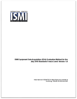
  1. ECCE Plus product- this software tool was originally developed under contract with the International Sematech Manufacturing Initiative (ISMI) to validate the fidelity, usability, and interoperability of early versions of the standard; it can used to manually execute a set of procedures documented in the “ISMI Equipment Data Acquisition (EDA) Evaluation Method for the July 2010 Standards Freeze Level: Version 1.0” document (see title page below) to exercise most of the capabilities called for in the standard; note that this is the only commercially available solution among the three.

ISMI.png

  1. Company-specific test suites – one major chip manufacturer (and early adopter of EDA) maintains its own partially-automated set of compliance tests, and provides this system to its equipment suppliers as a pre-shipment test vehicle. This set of tests is then used in the fab as part of the tool acceptance process; however, this system also includes a number of company-specific automation scenarios, which are not available for outside use. This highlights the need to support custom extensions in an industry-validated tester if it is to be commercially viable.

  2. In-house custom test clients – this is a variation of #2 that some of the major OEMs have chosen as their economies of scale dictate; the problems with this approach are that a) the test clients must be kept current with the EDA standards, which are themselves a moving target, and b) unless thoroughly validated by the eventual customers of the equipment, there is no guarantee that passing these tests will satisfy the final acceptance criteria for a given factory. 

For performance and stability testing, there are no automated solutions currently available. The ISMI EDA Evaluation Method does describe some rudimentary performance evaluation procedures, but these no longer reflect the expectations of the customers with many years of accumulated EDA production experience. Clearly a better solution is needed.

Finally, for metadata model conformance testing, the only available solution is the Metadata Conformance Analyzer (MCA) that was commissioned by Sematech and implemented by NIST (National Institute of Standards and Technology). It has not been updated in almost five years, and exhibits a number of known issues when applied to a SEMI E164-compliant equipment model (E164 = Specification for EDA Common Metadata), so it will be increasingly insufficient as more companies require full Freeze II / E164 specification compliance. 

The good news in all this is that Cimetrix has recognized and anticipated this emerging need, and is actively addressing it on our product roadmap. If you want to know more about EDA testing and/or discuss your specific needs, please contact Cimetrix for a demonstration of this exciting new capability!

Topics: EDA/Interface A, Data Collection/Management, Cimetrix Products, EDA Testing Series