by David Francis
Product Manager
Many years ago, I had the opportunity to work with some large semiconductor companies, including, Intel, Motorola, Lucent, and Siltronic. I developed interface acceptance tests for equipment they purchased. At that time, the SEMI SECS/GEM standards were still new and not widely adopted. Many of the tool vendors had little or no previous experience writing SECS/GEM interfaces, and they were often uncertain about the details of the standards, along with worrying about how they could comply with them. Chief among the vendors’ concerns was how they could meet their design schedules without loading down their engineering teams with this new requirement placed upon them.
Over the intervening years I worked in the scheduling and dispatching area of automated semiconductor manufacturing, and in that time I lost track of the SECS/GEM standards and their adoption by the wafer fabs.

Recently I joined Cimetrix as Product Manager for the connectivity and tool automation products, and now I am back in the world of SECS/GEM standards. A lot has changed since those early years, as fabs moved from 200mm to 300mm, and now considering 450mm wafer fabrication. In addition, the geometries have shrunk from 1 micron down to 40nm and below. However, I still see many of the same industry concerns as I did many years ago, even though there has been little change to the SECS/GEM standards.
The real change I see is the wide spread adoption of the SECS/GEM standard. Previously, only a few leading edge companies requested SECS/GEM interfaces on their tools and were working feverishly to set up host-side equipment controls. Today, SECS/GEM is well rooted in 300mm semiconductor manufacturing and tool vendors have very mature automation interfaces.
The move to 300mm processing created an ideal opportunity for the development and adoption of the GEM300 standards. Building new 300mm tools created an ideal environment for designing in the GEM300 standards right from the start.
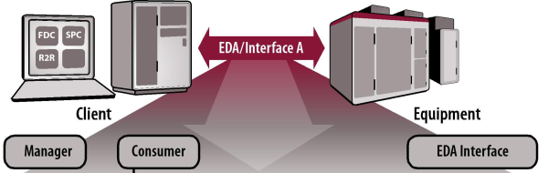
More recently, new standards, like Interface A, have emerged from their R&D phase and are now going through the same refining process that SECS/GEM went through a decade ago. These new standards will continue to support the industry’s efforts to create more efficient devices, at ever-decreasing geometries, with increased reliability and yield quality.
It is exciting to be working with these standards again and looking at them from the other end of the wire – the tool-side as opposed to my previous fab-side experience. I look forward to writing more about how the tool vendors are adopting, and demonstrating compliance, to the new standards.


 Fabs are like people, each one has it own personality traits. Fortunately, and arguably unfortunately, unlike people, most fabs have a handbook for their “personalities” in the form of specifications. I have found it interesting, that like people, fab “personalities” have common and unique features. Here are a few of examples:


